全网IC教育培训_一站式导航
收集整理全网IC教育培训资源,客服186-6709-0885
![[访谈-英飞凌]AI算力爆发,数据中心配电迎来“固态革命”——固态断路器如何千倍提速故障隔离?](https://material-image.wanwang.xin/1597234105050516/public/0061ea0b-5f32-4ec6-959d-140eb6e42d8f.png)
[访谈-英飞凌]AI算力爆发,数据中心配电迎来“固态革命”——固态断路器如何千倍提速故障隔离?
[访谈-英飞凌]AI算力爆发,数据中心配电迎来“固态革命”——固态断路器如何千倍提速故障隔离?
大纲 1. 开场:AI耗电狂飙,为何传统配电方案“顶不住了”? 2. 从AC到DC:光伏、电池、服务器全直流,减少转换损耗,电压升至400V/800V甚至1500V 3. 速度是王道:故障电流上升率可达500A/μs,机械断路器需10~20ms,固态方案只需微秒级,提速1000倍 4. 无火花、无噪声:固态断路器在电流刚上升时即切断,避免数十千安培的爆炸性电流 5. 并非全固态:仍需空气间隙实现安全隔离,但机械部分不再承担灭弧重任,体积更小、更耐用 6. 系统级挑战:多源汇流、层级保护、选择性协调——从单点对点到复杂DC微电网 7. 商业与标准化:初期成本高,但DC配电的价值主张明确;期待专用标准,规模效应将降低成本 8. 未来展望:电压向中压(34.5kV)延伸,市场百年未有之大变局,两年后格局将完全不同
完整版私信客服 186-6709-0885
![[SerDes]为什么接收机测试必须加入正弦波抖动(SJ)?——PCIe、以太网中的眼图应力与CDR跟踪揭秘](https://material-image.wanwang.xin/1597234105050516/public/555fc890-d549-4521-a93e-228c68a15005.png)
[SerDes]为什么接收机测试必须加入正弦波抖动(SJ)?——PCIe、以太网中的眼图应力与CDR跟踪揭秘
[SerDes]为什么接收机测试必须加入正弦波抖动(SJ)?——PCIe、以太网中的眼图应力与CDR跟踪揭秘
简介 本视频深入解析高速数字接收机测试中“正弦波抖动”(SJ)的核心作用。你会明白SJ并非模拟真实信号,而是作为一种可控、可重复的“时序标尺”,通过改变数据边沿的移动幅度和频率,精准测试接收机时钟数据恢复(CDR)电路的跟踪能力。视频涵盖PCIe、以太网等协议中的校准方法、抖动容限模板,以及SJ与信道损耗、随机抖动等其他损伤的配合。无论你是硬件工程师还是测试新手,这段讲解将帮你彻底理解为何合规性测试离不开SJ。
完整版私信客服 186-6709-0885
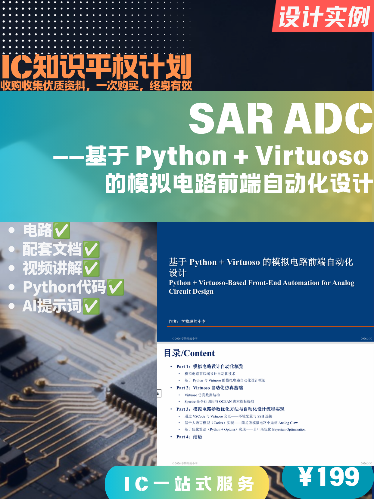
基于 Python + Virtuoso 的模拟电路前端自动化设计
基于 Python + Virtuoso 的模拟电路前端自动化设计
Part 1:模拟电路设计自动化概览 模拟电路前后端设计自动化技术 基于 Python 与 Virtuoso 的模拟电路自动化设计框架 Part 2:Virtuoso 自动化仿真基础 Virtuoso 仿真数据结构 Spectre 命令行调用与 OCEAN 脚本指标提取 Part 3:模拟电路参数优化方法与自动化设计流程实现 通过 VSCode 与 Virtuoso 交互——环境配置与 SSH 连接 基于大语言模型(Codex)实现——简易版模拟电路小龙虾 Analog Claw 基于优化算法(Python + Optuna)实现——贝叶斯优化 Bayesian Optimization Part 4:结语
完整版私信客服 186-6709-0885
![[曲博]蔡司如何成就EUV光刻?揭秘半导体制造背后的“光学巨人”](https://material-image.wanwang.xin/1597234105050516/public/3a36b612-f733-40b9-a132-dbf530b222a0.png)
[曲博]蔡司如何成就EUV光刻?揭秘半导体制造背后的“光学巨人”
[曲博]蔡司如何成就EUV光刻?揭秘半导体制造背后的“光学巨人”
简介 极紫外光(EUV)光刻机离不开荷兰ASML,但最关键的光学元件却来自德国蔡司。没有蔡司,就没有今天的先进制程。本期曲博科技教室,深入剖析蔡司在半导体制造中的全链路布局:从光罩修复、晶圆检测、3D封装失效分析,到高数值孔径EUV反射镜的极致工艺。AI时代晶片复杂度飙升,当结构小到“看不见”,蔡司如何用光学、精密量测和显微技术“看见良策”?内容涵盖隐藏缺陷检测、晶圆翘曲修复、交叉光束离子束切割等前沿技术,带你全面了解这家百年光学巨头如何突破科学极限,支撑起万亿半导体产业。
完整版私信客服 186-6709-0885
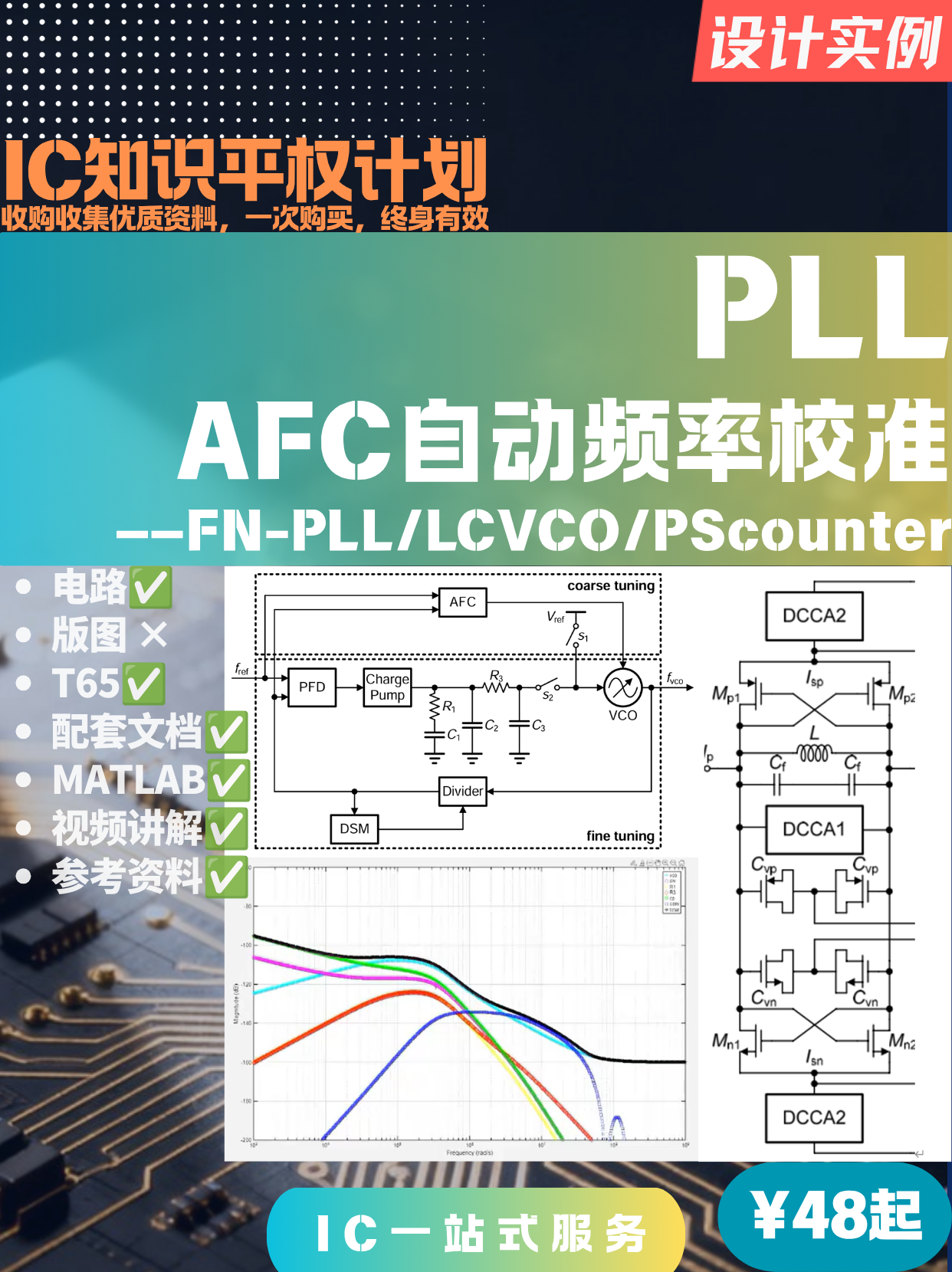
PLL-AFC自动频率校准——FN-PLL/LCVCO/PScounter
PLL-AFC自动频率校准——FN-PLL/LCVCO/PScounter
面向wifi频段的频率综合器 频率覆盖7.6-9.4GHz。 PFD:死区时间可控的三态PFD CP:电流可调舵电荷泵保证所想范围同时灵活调节电流。 LCVCO:带尾电流滤波的互补VCO确保高性能和低噪声。 DIV:基于吞脉冲的分频里搭配tspc逻辑和静态逻辑保证高速的同时兼顾低功耗。MASH1-1-1实现小数精度为24位的小数分频。 AFC功能模块保证初始阶段VCO的频带选择为最靠近目标频率。 顶层ams仿真均已通过。大量的trim设计 T65工艺【电路+复现的原博士论文档+视频讲解+MATLAB代码】
完整版私信客服 186-6709-0885
电路之美-拉扎维-20.从雷达到振荡器-如何用MOS制作雷达混频器
电路之美-拉扎维-20.从雷达到振荡器-如何用MOS制作雷达混频器
简介 在本期“电路之美”系列中,加州大学洛杉矶分校(UCLA)的Behzad Razavi教授带我们走进雷达的世界。从传统国防航空到现代自动驾驶,雷达已无处不在。但雷达究竟如何测量距离?如何用电路实现“时间延迟”的测量?Razavi教授从电磁波传播出发,推导出测距的核心 —— 相位差检测,并一步步展示如何用简单的MOSFET平方律特性构建乘法器(混频器),从而提取出我们想要的延迟信息。无需复杂数学,直观领略模拟电路的精妙设计。适合所有对射频、模拟IC和雷达系统感兴趣的工程师与学生。 --- 视频大纲 1. 雷达的现代应用 - 从机场塔台到车载避障、自动驾驶 - 测距的基本场景:轿车与卡车之间的距离测量 2. 测距原理 - 利用光速恒定,通过电磁波往返时间(延迟ΔT)计算距离 - 发射波与反射波的时间差 = 2×距离 / 光速 3. 数学建模 - 发射信号:A·sin(ω₀ t) - 反射信号:延迟后的正弦波,引入相位θ - θ与ΔT的关系,问题转化为“如何测量θ” 4. 乘法器 + 低通滤波方案 - 将发射波与接收波相乘,利用三角恒等式 - 产生:cos(θ)(低频,含延迟信息)和 cos(2ω₀ t + θ)(高频,可滤除) - 低通滤波器提取cos(θ),反推距离 5. 电路实现 —— MOSFET混频器 - MOSFET饱和区平方律特性:I_D ∝ (V_GS - V_TH)² - 将V₁(发射波)和V₂(接收波)相加后加至栅源 - 展开平方项,得到2·V₁·V₂ —— 自然实现乘法 - 滤波后得到所需相位信息 6. 总结与点睛 - 简洁而优雅的电路思想 - 从物理原理到晶体管级设计的完整链路 --- 关键词 雷达, 混频器, 乘法器, MOSFET, 平方律, 相位检测, 低通滤波, 测距, 射频电路, 自动驾驶, 模拟集成电路, 电磁波, Behzad Razavi
完整版私信客服 186-6709-0885
DC-DC模块电源选型与设计实战
DC-DC模块电源选型与设计实战
大纲 为什么要选择模块电源? 模块电源 vs 自研电源:优缺点全面对比 模块电源使用与设计核心技巧 模块电源并联问题深度解析 主流模块电源器件与购买渠道
完整版私信客服 186-6709-0885
【【IEEE研讨会】如何在IC企业中成为精英?-Dr. Chris Mangelsdorf
【【IEEE研讨会】如何在IC企业中成为精英?-Dr. Chris Mangelsdorf
在本期IEEE SSCS(固态电路协会)“青年卓越”网络研讨会中,我们非常荣幸地邀请到了Analog Devices(亚德诺半导体)前技术院士、MIT博士 Dr. Chris Mangelsdorf。Chris 结合自己在半导体行业四十余年的经验,深入剖析了年轻工程师在大型企业(如芯片公司)中常遇到的“隐形人”困境,并提出了两大核心技能:成为推动变革的“冠军” 与掌握有效的沟通艺术。 本次讲座不仅揭秘了企业资源分配和晋升的底层逻辑,更提供了具体可行的策略,帮助你在技术过硬的同时,提升个人“可见度”,获得应有的认可与职业发展。无论你是即将步入职场的学生,还是寻求突破的年轻职场人,这场分享都将为你提供宝贵的实战视角。
完整版私信客服 186-6709-0885

电路之美-拉扎维-19.从电话到红外线-手机如何“看见”你的耳朵?
电路之美-拉扎维-19.从电话到红外线-手机如何“看见”你的耳朵?
大纲 1. 手机如何感知“贴近耳朵”? - 红外发射器与屏幕自动关闭逻辑 - 从手机到电视遥控器的普遍应用 2. 红外发射端 —— LED如何产生不可见光 - PN结正向偏置:电子与空穴的注入 - 耗尽区内的复合过程与光子辐射 - 材料决定波长:可见光 vs. 红外光 3. 红外接收端 —— 光电二极管的工作原理 - 反向偏置下的光生电子-空穴对 - 光生电流的产生与模型(电流源等效) 4. 发射与接收的电路实现 - 发射端:MOSFET开关控制LED通断 - 接收端:光电二极管 + 低输入阻抗放大器(Miller效应回顾) 5. 关键挑战:如何抵抗环境光干扰? - 环境光(含红外成分)对接收器的误触风险 - 解决方案:调制 —— 用数据比特流控制LED闪烁 - 接收端解调恢复原始数字信号 6. 进阶应用:Face ID中的红外点阵投影 - 黑暗中如何识别面部? - 单颗红外LED快速扫描投影30,000个点 - 通过反射点阵重建面部深度与轮廓,实现解锁 7. 总结 - 从基础物理到尖端产品的完整链路 - 红外技术的优雅与实用之美
完整版私信客服 186-6709-0885

1nm以下制程关键突破!台积电联手阳明交大,解决二维材料"散射"难题,让电子跑更快!
1nm以下制程关键突破!台积电联手阳明交大,解决二维材料"散射"难题,让电子跑更快!
半导体巨头台积电与阳明交通大学合作,在国际知名期刊《自然·电子学》(Nature Electronics)上发表了一项关键突破。随着先进制程迈向1纳米以下,传统的硅材料已逼近物理极限,二维材料(如二硫化钼)被视为重要的替代方案。 然而,二维材料与高介电常数(High-k)绝缘层(如氧化铪)的结合,会产生严重的散射效应,导致电子移动速度(载子迁移率)大幅下降。本次研究中,科学家们通过在二硫化钼(MoS₂)和氧化铪(HfO₂)之间,插入一层利用磊晶工艺衍生的超薄氧化铝(Al₂O₃)界面层,成功解耦了通道与介电层的直接作用,有效抑制了散射。 借助该技术,团队成功制作出通道长度约100纳米(未来可微缩至10纳米以下)的顶部栅极晶体管,在等效氧化层厚度(EOT)约1纳米的条件下,实现了每微米0.45毫西门子(mS/μm)的高跨导,为未来超大规模集成电路的二维材料应用铺平了道路。
完整版私信客服 186-6709-0885
![[Digikey]2026.08多相BUCK/BOOST电源技术深度解析](https://material-image.wanwang.xin/1597234105050516/public/f345e80e-0f87-4376-a66e-b5b42ffb450f.png)
[Digikey]2026.08多相BUCK/BOOST电源技术深度解析
[Digikey]2026.08多相BUCK/BOOST电源技术深度解析
大纲 AI时代的供电挑战 核心供电架构:从48V到负载点(VRM) 关键技术一:DRMOS(集成驱动MOSFET) 关键技术二:多相交错并联BUCK 技术延伸:多相交错并联BOOST 总结与相关器件介绍
完整版私信客服 186-6709-0885
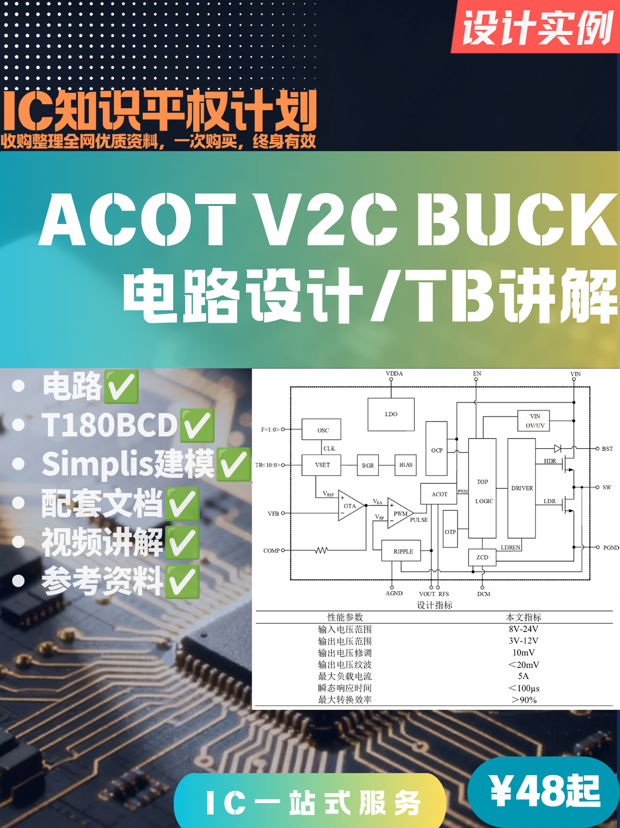
【设计实例】ACOT V2C BUCK电路
【设计实例】ACOT V2C BUCK电路
发货内容: 1、完整BUCK电路-TOP-DOWN,+PDK(BCD工艺) 2、30页PDF文档,1W字以上分析(理论分析,电路介绍,部分仿真结果) 3、简要原理概述+TB设计讲解 4、参考资料 性能: 输入最高24V电压,最大5A负载电流(可拓展),输出电压可修调,软启,DCM/FCCM切换,自适应Ton可修调,最小Toff时间,纹波补偿,各类保护电路。
完整版私信客服 186-6709-0885
无片外电容型LDO(Capless LDO)架构介绍、优势与核心挑战解析
无片外电容型LDO(Capless LDO)架构介绍、优势与核心挑战解析
本视频文稿围绕全片上集成的无输出电容LDO(即无片外电容LDO)架构展开,首先说明该架构的定义,随后梳理其无需外部引脚、物料成本低、占用面积小、无需短路保护、启动电路简单等核心优势,同时也指出其存在负载与线性瞬态响应差、设计复杂度高的权衡点,最后重点拆解了瞬态响应差的成因并通过量化计算验证片上电容补足的局限性,同时明确了该架构设计复杂度高的四大具体成因。
完整版私信客服 186-6709-0885
AI 会取代模拟电路设计师吗?——Behzad Razavi 教授的深度剖析
AI 会取代模拟电路设计师吗?——Behzad Razavi 教授的深度剖析
00:00 开场介绍 02:59 演讲框架与AI五级金字塔 07:02 评估一:分析能力测试(ChatGPT vs Gemini) 13:40 评估二:趋势预测(Gemini 3.1 Pro) 29:03 训练AI的挑战与拓扑爆炸 34:29 AI黑箱问题与调试困境 37:00 创新:AI能否做到? 41:55 结论与总结 43:24 Q&A互动环节
完整版私信客服 186-6709-0885
PCIe接收端测试中的DMSI:2.1GHz差模正弦干扰的原理与验证方法
PCIe接收端测试中的DMSI:2.1GHz差模正弦干扰的原理与验证方法
本视频深入解析PCIe合规性测试中的关键项目——差模正弦干扰(DMSI/DMI)。我们将探讨为什么PCI-SIG要在数据信号上叠加2.1GHz的差分正弦波,这种干扰如何影响接收端眼图,以及哪些电路模块对DMSI最为敏感。内容涵盖DMSI的测试设置原理、与CDR和DFE的相互作用机制,以及如何在流片前通过线性传输检查、瞬态眼图仿真和闭环验证三种方法来确保设计裕量。无论您是高速SerDes设计工程师还是信号完整性工程师,都能从中获得实用的验证思路。
完整版私信客服 186-6709-0885

模拟IC工程师如何实际解决短沟道效应2026
模拟IC工程师如何实际解决短沟道效应2026
本视频深入讲解亚100纳米CMOS晶体管中两项关键器件工程技术——Halo(晕环/口袋)注入与轻掺杂漏极(LDD)的物理本质。区别于单纯的工艺流程描述,本课程从静电学第一性原理出发,剖析电荷共享、漏致势垒降低(DIBL)、热载流子注入(HCI)等核心问题的物理机制,并演示如何通过掺杂分布设计来精确调控电势分布。内容涵盖:短沟道效应的Poisson方程解读、Halo注入如何抑制DIBL与VT滚降、LDD结构对峰值电场的调控、侧墙(Spacer)的多重功能,以及完整掺杂分布的设计层次。适合具备半导体物理基础、希望建立器件工程师系统思维的观众。
完整版私信客服 186-6709-0885
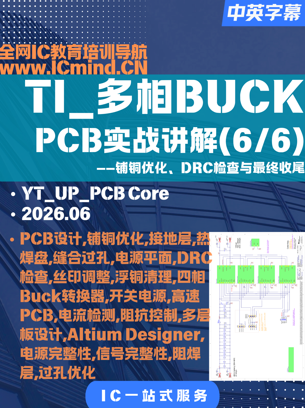
TI_多相BUCK_PCB设计实战6/6:从电容配置到信号布线的完整设计流程
TI_多相BUCK_PCB设计实战6/6:从电容配置到信号布线的完整设计流程
本视频详细演示了一款多相降压电源转换器的PCB布局设计全过程。内容涵盖输出电容组的优化配置、多边形铜皮的创建与合并技巧、过孔缝合策略、同步信号与使能信号的菊花链布线,以及电流检测、反馈网络等关键信号的走线方法。重点讲解了在紧凑空间内平衡功率回路低电感设计与信号完整性的工程取舍,包括层叠规划、接地处理和网络分析仪注入端口的差分对布线等实用技术。
完整版私信客服 186-6709-0885
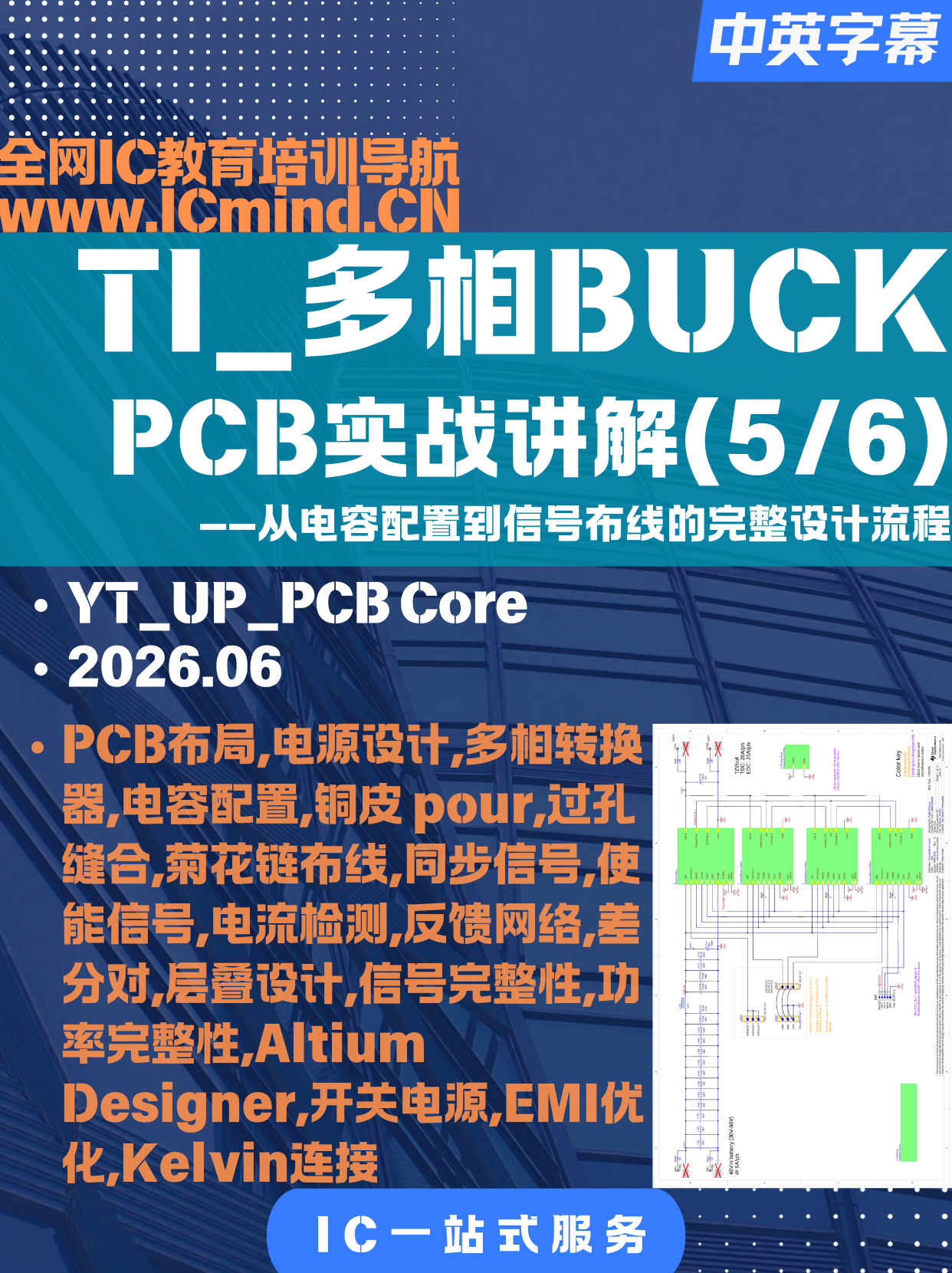
TI_多相BUCK_PCB设计实战5/6::从电容配置到信号布线的完整设计流程
TI_多相BUCK_PCB设计实战5/6::从电容配置到信号布线的完整设计流程
本视频详细演示了一款多相降压电源转换器的PCB布局设计全过程。内容涵盖输出电容组的优化配置、多边形铜皮的创建与合并技巧、过孔缝合策略、同步信号与使能信号的菊花链布线,以及电流检测、反馈网络等关键信号的走线方法。重点讲解了在紧凑空间内平衡功率回路低电感设计与信号完整性的工程取舍,包括层叠规划、接地处理和网络分析仪注入端口的差分对布线等实用技术。
完整版私信客服 186-6709-0885
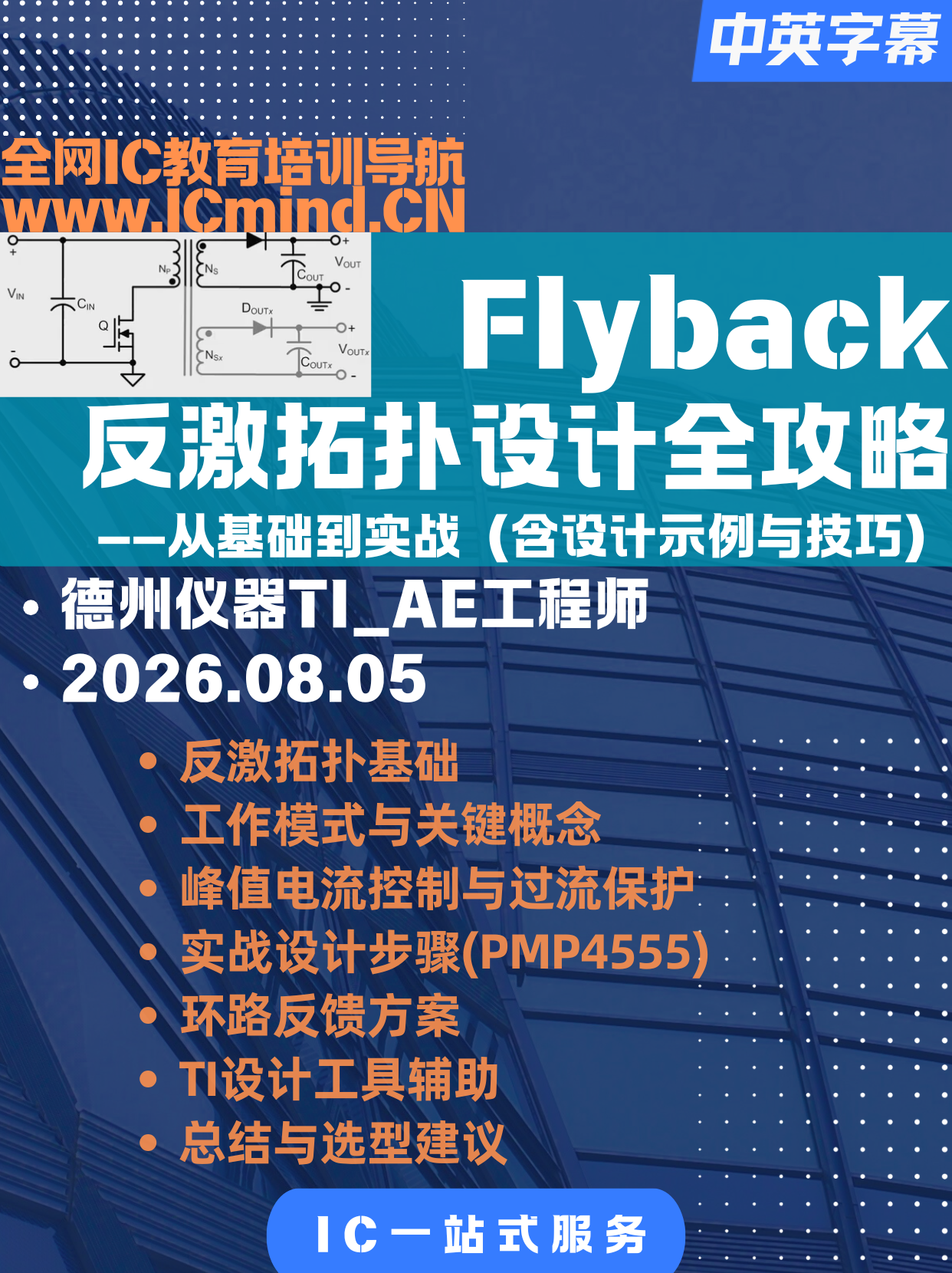
TI_Flyback反激拓扑设计全攻略
TI_Flyback反激拓扑设计全攻略
反激拓扑基础 工作模式与关键概念 峰值电流控制与过流保护 实战设计步骤(PMP4555) 环路反馈方案 TI设计工具辅助 总结与选型建议
完整版私信客服 186-6709-0885

电路之美-拉扎维-18从数据中心到米勒效应
电路之美-拉扎维-18从数据中心到米勒效应
本视频深入解析数据中心内部机架间高速光通信的核心技术。从光电二极管的基本工作原理出发,揭示传统电阻负载方案面临的RC时间常数限制与带宽瓶颈。重点讲解如何运用米勒定理设计跨阻放大器(TIA),在不牺牲输出电压摆幅的前提下,将等效输入电阻降低(1+A)倍,从而显著提升电路带宽。通过CMOS反相器实现的实际设计案例,展示从6.4 GHz到22 GHz的带宽提升效果,阐述高速光接收前端的关键设计考量。
完整版私信客服 186-6709-0885
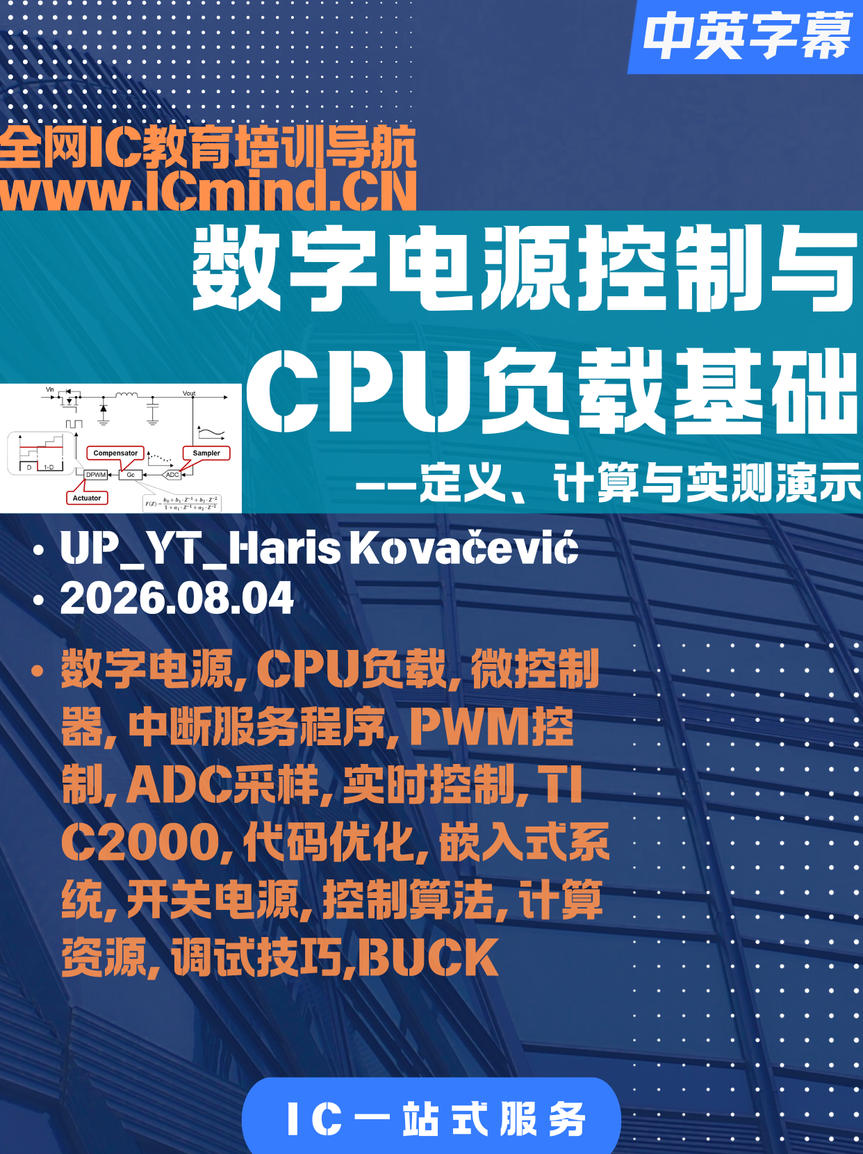
数字电源控制中的CPU负载基础:定义、计算与实测演示
数字电源控制中的CPU负载基础:定义、计算与实测演示
本视频是"CPU负载与数字电源实时软件设计"系列的第一集,面向嵌入式控制工程师讲解数字电源控制中的核心概念——CPU负载。视频首先解释了在200kHz开关频率下,微控制器仅有5微秒完成采样、控制算法执行和PWM更新的时间压力;接着通过时序图详细定义了CPU负载的计算方法(中断执行时间与中断周期之比);最后以TI C2000微控制器控制的同步Buck变换器为实例,演示如何使用示波器通过GPIO翻转测量实际的CPU负载(本例中为30%)。本系列将从基础概念逐步深入到代码优化与实时软件设计实践。
完整版私信客服 186-6709-0885
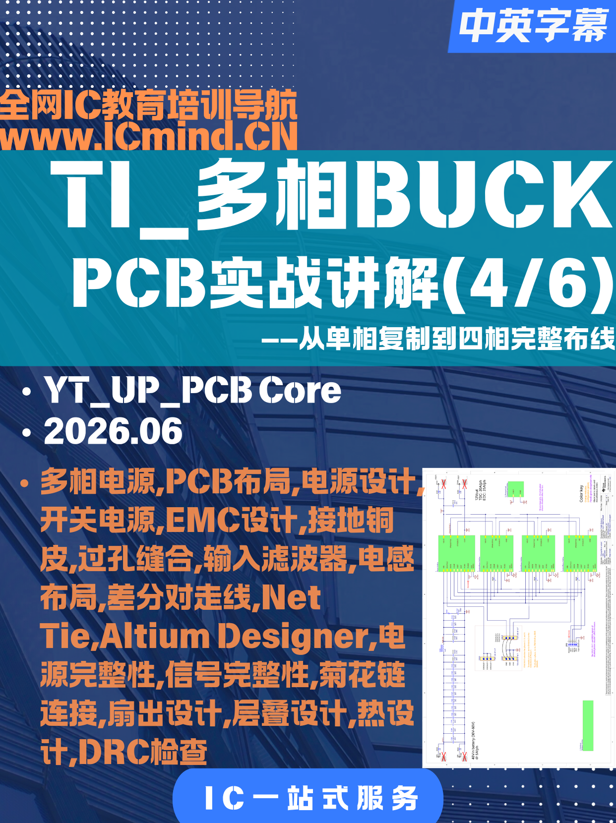
TI_多相BUCK_PCB设计实战4/6:从单相复制到四相完整布线
TI_多相BUCK_PCB设计实战4/6:从单相复制到四相完整布线
本视频详细演示了一款多相电源控制器的PCB布局设计全过程。内容涵盖从单相电路的基础布局开始,逐步扩展到四相设计的完整复制流程。重点讲解了关键信号(IMON、ISET、VSET)的扇出与菊花链连接、输入滤波器的优化放置、接地铜皮的分层管理、以及电感下方禁铺铜等EMC设计要点。同时展示了如何利用多相复制技术提高效率,并处理层间缝合过孔、差分对走线、Net Tie布局等细节问题。适合有一定基础的硬件工程师和PCB设计人员学习参考。
完整版私信客服 186-6709-0885
![[DAC]从理论到制造Gabriela Manganaro教授](https://material-image.wanwang.xin/1597234105050516/public/eabd6e23-71c3-4b91-81bb-5989efb3ef52.png)
[DAC]从理论到制造Gabriela Manganaro教授
[DAC]从理论到制造Gabriela Manganaro教授
本视频为Gabriela Manganaro教授主讲的《多GS/s奈奎斯特DAC:从理论到芯片》课程概览。该课程共8讲,每讲2小时,将于今年9月开课。课程涵盖高速高精度DAC设计的完整知识体系:从信号处理基础、多层级建模技术,到电流舵DAC核心架构及电荷分配型、反相器型等替代方案;深入剖析制造非理想性、电路失配、布局寄生等关键问题及其对频谱性能的影响;系统讲解动态元件匹配、前台/后台校准、交错式DAC校准等误差消除技术;并结合GlobalFoundries 22nm FDX工艺的两个实战案例(14bit 1GS/s无线应用DAC与7bit 28GS/s有线通信交错DAC),通过两次实践环节传授仿真策略与调试技巧。适合具备模拟IC设计基础、希望掌握多GS/s DAC从系统架构到物理实现全流程的工程师与研究人员。
完整版私信客服 186-6709-0885
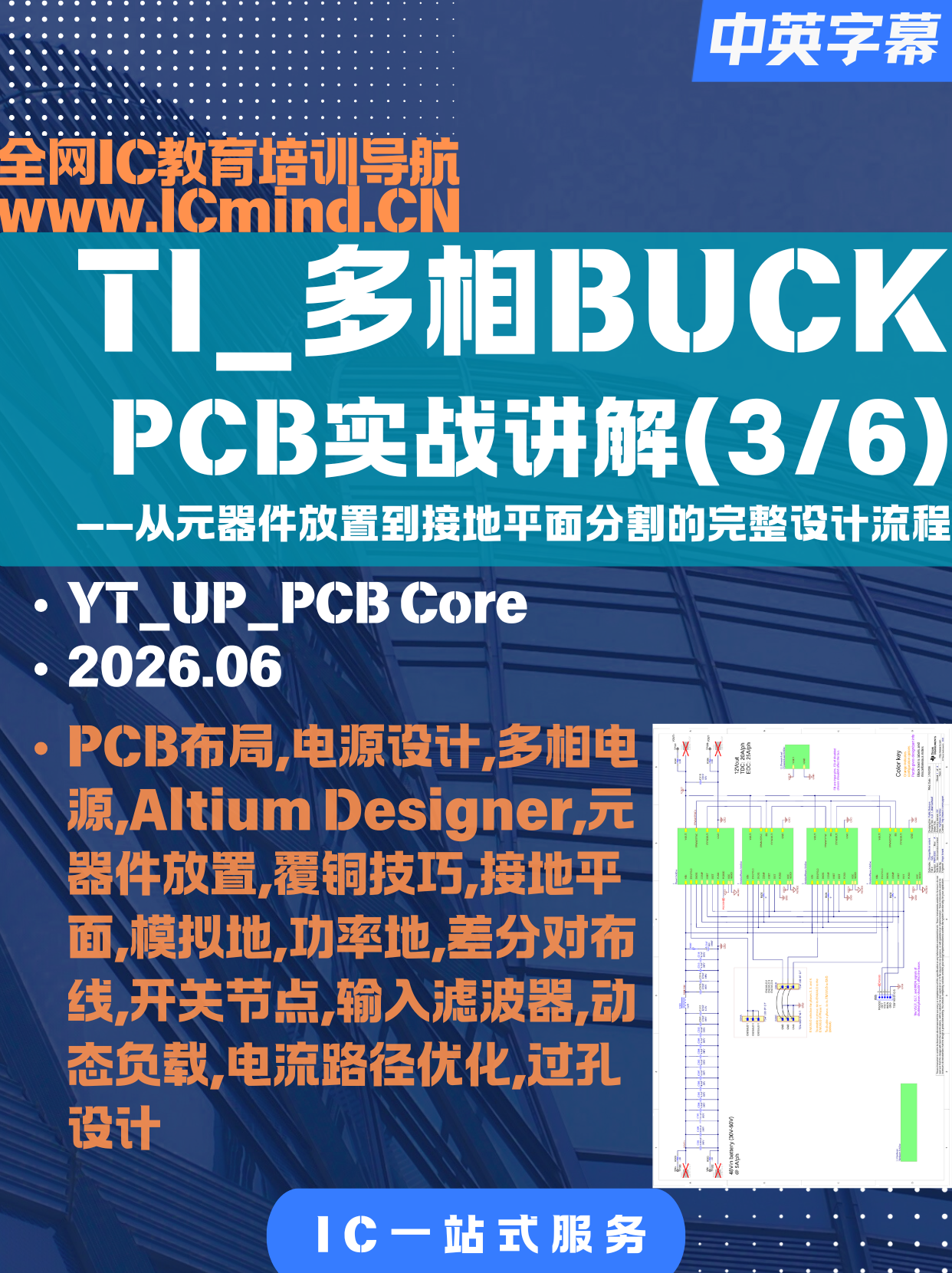
TI_多相BUCK_PCB设计实战3/6::从元器件放置到接地平面分割的完整设计流程
TI_多相BUCK_PCB设计实战3/6::从元器件放置到接地平面分割的完整设计流程
本视频详细演示了一个四相电源PCB的完整布局过程。内容涵盖跳线电阻放置、动态负载电路布局、输入滤波器设计、多相功率路径规划等关键环节。重点讲解了如何利用多边形覆铜优化电流路径、处理开关节点布线、以及模拟地与功率地的分割策略。视频还分享了实用的Altium Designer操作技巧,包括快捷键设置、差分对布线、过孔放置优化等,适合有一定基础的PCB设计工程师参考学习。
完整版私信客服 186-6709-0885
高速串行接收机中的采样器回踢效应:从电路细节到系统架构问题
高速串行接收机中的采样器回踢效应:从电路细节到系统架构问题
本视频深入探讨高速串行通信接收机中的采样器回踢(Kickback)效应。不同于传统认知中将其视为单纯的比较器问题,本视频重点分析回踢如何在串联接收机架构中演变为系统级问题——影响数据眼图、时钟数据恢复(CDR)和判决反馈均衡(DFE)。内容涵盖回踢的产生机理(积分阶段与判决阶段的共同贡献)、快速评估方法(初始电压阶跃与建立时间估算)、对PAM4调制的影响、以及CDR锁定点偏移和相位检测器增益变化等关键问题。最后提供完整的仿真验证方法与工程实践建议,帮助设计者准确评估回踢是否会成为架构级瓶颈。
完整版私信客服 186-6709-0885
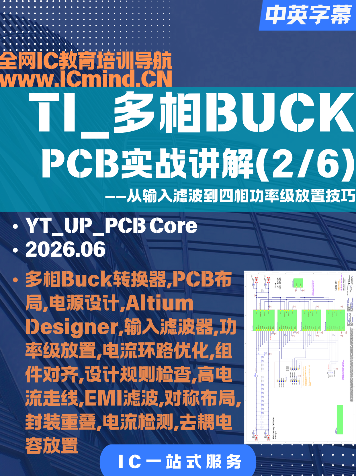
TI_多相BUCK_PCB设计实战2/6:从输入滤波到四相功率级放置技巧
TI_多相BUCK_PCB设计实战2/6:从输入滤波到四相功率级放置技巧
本视频详细演示了多相Buck转换器PCB布局的完整流程,重点讲解如何合理规划电路板空间。内容涵盖输入EMI滤波器的放置策略、连接器位置优化、四相功率级的对称布局方法,以及如何处理高电流路径的走线规划。工程师将分享实用的布局技巧,包括使用Altium Designer进行组件对齐、创建参考特征点实现精确定位、处理重叠封装的设计规则设置,以及如何在有限空间内优化电流环路。视频还讨论了顶层/底层组件分配、电流检测电阻布置等关键考量因素,适合电源硬件工程师和PCB布局工程师学习参考。
完整版私信客服 186-6709-0885
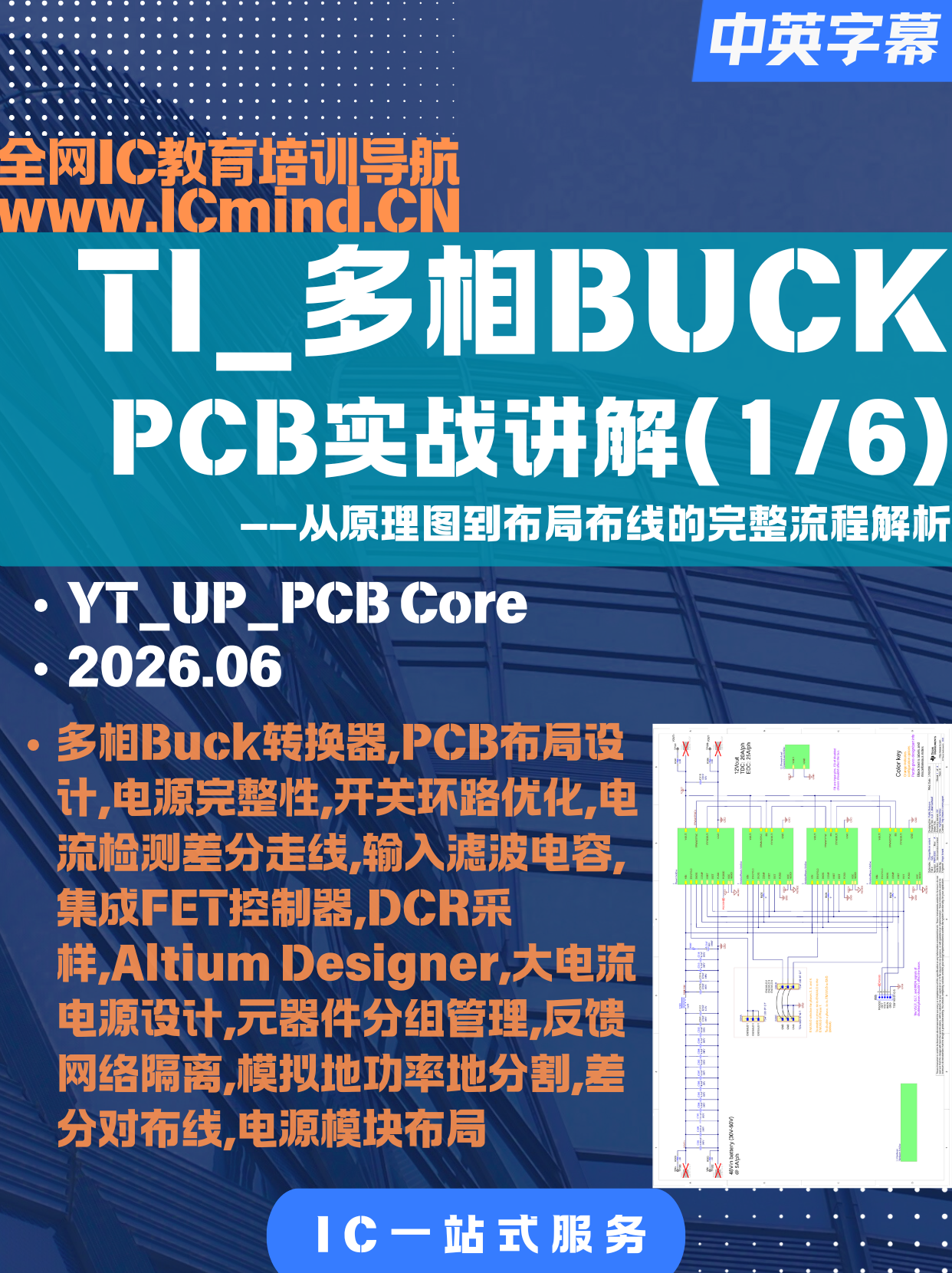
TI_多相BUCK_PCB设计实战1/6:从原理图到布局布线的完整流程解析
TI_多相BUCK_PCB设计实战1/6:从原理图到布局布线的完整流程解析
本视频详细演示了如何基于TI参考设计完成一款多相Buck电源板的PCB设计。内容涵盖原理图解读、元器件分组管理、输入滤波电容布局优化、开关环路最小化设计、电流检测差分走线、反馈网络隔离等关键技术要点。设计师以四相80-100A输出的大电流电源为例,展示了从初始元件放置、密度优化到底层元件布局的完整迭代过程,并分享了处理集成FET控制器、DCR电流采样、模拟地与功率地分割等实际工程经验。适合有一定基础的硬件工程师和PCB Layout工程师学习参考。
完整版私信客服 186-6709-0885

【电路之美-拉扎维-17】从互联网到MUX-光纤通信与多路复用技术:数据如何穿越美国
【电路之美-拉扎维-17】从互联网到MUX-光纤通信与多路复用技术:数据如何穿越美国
本视频由著名电路设计专家Behzad Razavi教授主讲,深入解析互联网数据传输的核心原理。从洛杉矶到纽约的远距离数据通信如何实现?为什么我们需要光纤而非铜缆?视频从基础的多路复用(Multiplexing)技术讲起,通过2选1开关电路的直观演示,逐步扩展到千级用户的多路复用树架构。详细讲解电光转换(激光二极管)、光纤传输、光电转换(光电二极管)的完整链路,揭示100Gbps高速数据传输背后的电路设计之美。适合通信工程、电子工程专业的学生和工程师学习。
完整版私信客服 186-6709-0885
混合CDR架构:为何不必在模拟与数字之间二选一
混合CDR架构:为何不必在模拟与数字之间二选一
本视频深入解析混合时钟数据恢复(Hybrid CDR)架构的设计哲学。我们回顾了纯模拟CDR和纯数字CDR各自的优缺点——模拟CDR速度快、延迟低、时间控制精细但难以编程和监控;数字CDR易于编程、参数可调但存在延迟、功耗和频率分辨率等问题。混合CDR的核心思想并非简单折中,而是根据每个功能的需求选择最佳实现方式:将快速、噪声敏感、低延迟的功能保留在模拟域,将慢速控制、积分、校准和监控功能移至数字域。视频详细讲解了经典混合CDR的双路径架构(快速模拟比例路径+慢速数字积分路径),分析了其五大优势,并探讨了实际应用中的多种混合形式。同时,我们也坦诚讨论了混合架构带来的设计挑战,包括路径间交互、量化效应、PVT变化以及模式切换平滑性等关键问题。最终结论是:混合CDR是一种 deliberate 的设计方法论——不为模拟或数字之名而选择,而是为每个功能选择最合适的实现方式。
完整版私信客服 186-6709-0885
![[SerDes]混合CDR架构:为何不必在模拟与数字之间二选一](https://material-image.wanwang.xin/1597234105050516/public/c64cf9d0-db20-429a-8aee-7925f9f2f9a3.png)
[SerDes]混合CDR架构:为何不必在模拟与数字之间二选一
[SerDes]混合CDR架构:为何不必在模拟与数字之间二选一
本视频深入解析混合时钟数据恢复(Hybrid CDR)架构的设计哲学。我们回顾了纯模拟CDR和纯数字CDR各自的优缺点——模拟CDR速度快、延迟低、时间控制精细但难以编程和监控;数字CDR易于编程、参数可调但存在延迟、功耗和频率分辨率等问题。混合CDR的核心思想并非简单折中,而是根据每个功能的需求选择最佳实现方式:将快速、噪声敏感、低延迟的功能保留在模拟域,将慢速控制、积分、校准和监控功能移至数字域。视频详细讲解了经典混合CDR的双路径架构(快速模拟比例路径+慢速数字积分路径),分析了其五大优势,并探讨了实际应用中的多种混合形式。同时,我们也坦诚讨论了混合架构带来的设计挑战,包括路径间交互、量化效应、PVT变化以及模式切换平滑性等关键问题。最终结论是:混合CDR是一种 deliberate 的设计方法论——不为模拟或数字之名而选择,而是为每个功能选择最合适的实现方式。
完整版私信客服 186-6709-0885
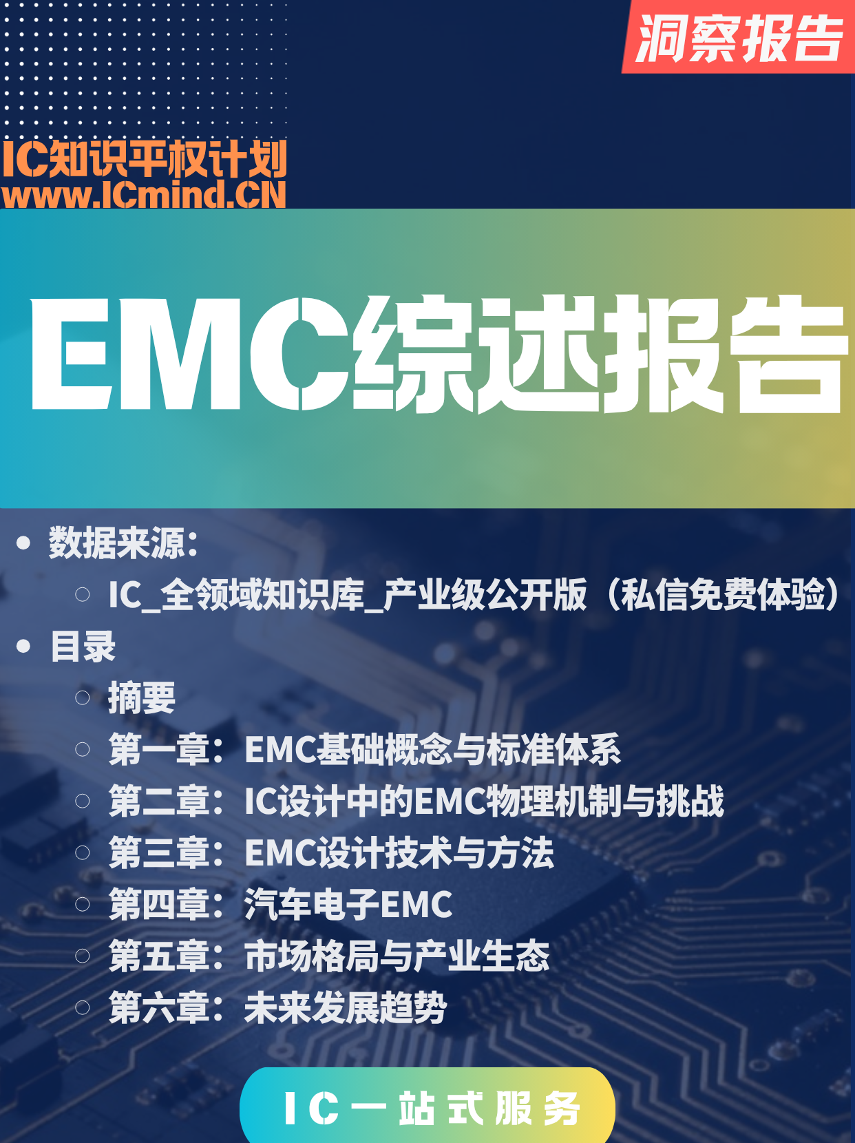
EMC综述报告
EMC综述报告
数据来源: IC_全领域知识库_产业级公开版(私信186-6709-0885免费体验) 目录 摘要 第一章:EMC基础概念与标准体系 第二章:IC设计中的EMC物理机制与挑战 第三章:EMC设计技术与方法 第四章:汽车电子EMC 第五章:市场格局与产业生态 第六章:未来发展趋势
完整版私信客服 186-6709-0885
AI数据中心电源解决方案:从电网到GPU的完整技术布局
AI数据中心电源解决方案:从电网到GPU的完整技术布局
本视频由意法半导体专家David Kudelásek主讲,全面展示ST面向AI数据中心的完整电源产品组合。内容涵盖三大核心板块:AC-DC前端电源(8.4kW/5.5kW参考设计)、800V高压直流输电的三种DC-DC架构(集中式边车、机架集中式、本地化模块化方案),以及液冷散热系统(4kW/7kW/10kW热泵驱动方案)。重点解析碳化硅、氮化镓与硅技术的最优组合如何实现高效率、高功率密度与电网稳定性,满足超大规模数据中心严苛的能效与设计规范。
完整版私信客服 186-6709-0885
【电路之美-拉扎维-16】从USB到放大器-USB高速传输的秘密:均衡器如何拯救信号失真
【电路之美-拉扎维-16】从USB到放大器-USB高速传输的秘密:均衡器如何拯救信号失真
本视频深入解析USB电缆在高速数据传输中面临的挑战。从USB 2.0的480 Mbps到USB 4的40 Gbps,传输速度的飞跃带来了信号衰减问题——高频分量在电缆中严重损耗,导致数据波形畸变、难以识别。视频详细讲解了均衡器(Equalizer)的工作原理:通过电容退化的共源级电路,在接收端补偿高频衰减,实现频率响应的平坦化。针对更长电缆的更严重衰减,还介绍了级联多级均衡器的解决方案。适合电子工程学习者、硬件设计工程师及对高速信号完整性感兴趣的观众。
完整版私信客服 186-6709-0885

MIT 突破1000TBs芯片:英伟达的真正噩梦?光互连技术如何颠覆AI算力格局
MIT 突破1000TBs芯片:英伟达的真正噩梦?光互连技术如何颠覆AI算力格局
MIT研究团队正在攻关1皮比特每秒(petabit/s)的光互连芯片技术,速度相当于每秒传输1000太比特数据。本视频深入解析这项名为FUTUR-IC的项目核心——"光学焊点"(optical solder bumps)技术,探讨它为何可能动摇英伟达在AI数据中心领域的护城河。我们将客观分析:光互连 vs 电互连的优劣、技术落地的真实挑战、英伟达的应对策略,以及这项技术对AI能耗危机的深远意义。这不是简单的"实验室突破"炒作,而是一次关于计算基础设施未来走向的深度思考。
完整版私信客服 186-6709-0885
英飞凌&马德里大学-多相LLC变换器小型化技术:航空应用中的高功率密度DC-DC转换解决方案
英飞凌&马德里大学-多相LLC变换器小型化技术:航空应用中的高功率密度DC-DC转换解决方案
本次研讨会由马德里大学的Daniel Rias主讲,深入探讨了面向航空应用的多相LLC谐振变换器小型化设计方法。演讲内容涵盖了从270V高压直流到28V低压直流的宽输入电压范围DC-DC转换技术挑战,重点介绍了三相LLC拓扑相比传统单相方案在功率密度提升方面的优势。主讲人详细阐述了Y-Δ变压器配置、磁集成设计、PCB布局优化、ZVS软开关实现以及GaN器件应用等关键技术,并分享了AltGain项目中的实验验证结果,最终实现了超过96%的转换效率和35-40kW/L的功率密度目标。本报告为高性能航空电源变换器的设计提供了系统性的工程实践指导。
完整版私信客服 186-6709-0885
【电路之美-拉扎维-15】从笔记本电脑到二极管,CPU温度监测的奥秘:芯片内置温度计电路设计
【电路之美-拉扎维-15】从笔记本电脑到二极管,CPU温度监测的奥秘:芯片内置温度计电路设计
**视频标题:** 笔记本电脑CPU温度监测的奥秘:芯片内置温度计电路设计 **视频简介:** 本视频由著名电路设计专家Behzad Razavi教授讲解笔记本电脑处理器(CPU)的温度监测原理。视频首先解释了CPU时钟频率与温度之间的关系——当运行视频流、游戏等高负载应用时,CPU频率升高导致功耗增加,数百万个内部节点同时对寄生电容充放电,产生大量热量。由于环境温度变化的影响,无法简单通过限制频率来控制温度,因此需要在芯片上集成温度计电路。Razavi教授详细推导了利用两个相同二极管在不同电流下的电压差(ΔV_BE)来产生与绝对温度成正比(PTAT)的电压信号,该信号经模数转换后用于动态调节CPU频率,防止芯片过热损坏。这是一个将模拟电路精巧设计应用于实际工程问题的经典案例。 **关键词:** CPU温度监测,芯片内置温度计,PTAT电路,二极管温度传感器,热电压,模拟集成电路设计,动态频率调节,功耗管理,寄生电容,模数转换,Behzad Razavi,电路设计,半导体器件,温度补偿,过热保护
完整版私信客服 186-6709-0885

数据中心AI供电:从48V到800V-常见问题
数据中心AI供电:从48V到800V-常见问题
简介 AI算力需求疯狂增长,机柜功耗飙升至百万瓦级!传统的48V供电系统因电流过大,面临铜线粗如大腿、发热严重、能源效率低下的物理瓶颈。 辉达(NVIDIA)在2025年COMPUTEX宣布,将联手供应链在2027年推行800V高压直流架构,彻底改写数据中心供电逻辑。本视频将用通俗易懂的物理原理,为你拆解: 1. 为什么提高电压能解决“大象级”的发热难题? 2. 为什么一定要用直流电?交流电在机房输配中吃了多少亏? 3. 800V落地竟要感谢电动车?碳化硅(SiC) 和氮化镓(GaN) 为何成为关键拼图? 4. 高压直流带来的致命杀手——“直流电弧”是什么?固态断路器如何用半导体魔法驯服它? 5. 高压不解决散热?揭秘液冷+800V在超高密度机柜(如NVL144)中的角色。 这是算力暴增时代的物理必修课,带你提前看懂下一代AI基础设施!
完整版私信客服 186-6709-0885
【电路之美-拉扎维-14】手机相机传感器的工作原理:从光子到数字图像
【电路之美-拉扎维-14】手机相机传感器的工作原理:从光子到数字图像
本视频由知名电路设计专家Behzad Razavi教授讲解,深入剖析智能手机相机内部的核心技术。视频从像素阵列的基本结构出发,详细解释光电二极管如何将光信号转换为电信号,以及源极跟随器缓冲电路的作用。重点探讨了模数转换器(ADC)的设计挑战:为什么不能在每个像素放置一个ADC?为什么也不能让所有像素共享一个ADC?最终揭示现代CMOS图像传感器采用的"列并行ADC"架构——在芯片面积、功耗和转换速度之间取得完美平衡的工程智慧。
完整版私信客服 186-6709-0885
![[SerDes]为什么模拟CDR(Bang-Bang CDR)至今仍是经典选择?深入解析其架构优势与适用场景](https://material-image.wanwang.xin/1597234105050516/public/768795a0-2cfa-454b-ac9c-179314cd67bc.png)
[SerDes]为什么模拟CDR(Bang-Bang CDR)至今仍是经典选择?深入解析其架构优势与适用场景
[SerDes]为什么模拟CDR(Bang-Bang CDR)至今仍是经典选择?深入解析其架构优势与适用场景
本视频深入探讨模拟Bang-Bang CDR(时钟数据恢复电路)的核心架构原理及其数十年长盛不衰的原因。我们将从CDR的基本功能出发,详细解析传统模拟CDR的组成部分:相位检测器、电荷泵、RC环路滤波器和压控振荡器(VCO)。重点阐述Bang-Bang相位检测器的三大特性——简单性、鲁棒性和快速响应,以及模拟CDR的三大核心优势:零环路延迟、实现简洁性和经过验证的高速性能。视频还将明确界定模拟CDR的最佳适用场景:中等数据速率、稳定信道、少量链路、有限可编程性需求的系统。同时预告后续内容,将讨论现代复杂系统(多链路、宽PVT变化、动态信道、背景校准需求)中模拟CDR面临的挑战。无论你是高速接口设计工程师还是学习SerDes技术的初学者,本视频都将帮助你建立对经典CDR架构的系统性认知。
完整版私信客服 186-6709-0885
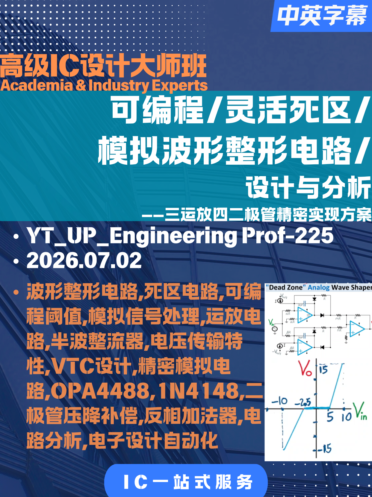
可编程灵活死区模拟波形整形电路设计与分析 | 三运放四二极管精密实现方案
可编程灵活死区模拟波形整形电路设计与分析 | 三运放四二极管精密实现方案
本视频详细讲解一种创新的模拟波形整形电路,该电路采用三运放和四二极管的巧妙结构,实现具有可编程灵活死区的电压传输特性(VTC)。视频分为三个部分:首先深入剖析电路工作原理,包括三个子电路(两个互补半波整流器和一个反相加法器)的协同作用;其次推导输出电压与输入电压的通用公式,详细讲解四个关键参数(α、β、M、N)如何独立控制死区阈值和象限斜率,并以具体实例(死区-2.5V至+5V,斜率分别为2和3)完成元件参数计算;最后讨论实际设计考量,包括运放选型(推荐OPA4488/OPA1656)、1%精密电阻选择、稳定性补偿电容配置,以及1N4148二极管正向压降对电路性能的影响。本电路通过预偏置电流技术实现精确的阈值控制,且输出特性与二极管实际压降无关,是精密模拟信号处理的优秀解决方案。
完整版私信客服 186-6709-0885
【电路之美-拉扎维-13】从心脏到运放:心脏信号检测电路设计:从生物电信号采集到噪声消除的完整解决方案
【电路之美-拉扎维-13】从心脏到运放:心脏信号检测电路设计:从生物电信号采集到噪声消除的完整解决方案
**视频标题:** 心脏信号检测电路设计:从生物电信号采集到噪声消除的完整解决方案 **视频简介:** 本视频由著名电路设计专家Behzad Razavi教授主讲,深入讲解心电图(ECG)信号检测电路的设计原理。内容涵盖:人体心电信号的产生机制与波形特征、高阻抗皮肤接触带来的信号衰减问题、非反相放大器拓扑的选择依据、以及最关键的差分放大技术——如何通过双电极采集消除60Hz工频干扰噪声。适合电子工程、生物医学工程专业的学生和工程师学习参考。 **关键词:** 心电图,ECG,生物电信号,仪表放大器,差分放大,共模抑制,60Hz噪声,工频干扰,输入阻抗,心电检测电路,模拟前端,信号调理,Behzad Razavi,电路设计
完整版私信客服 186-6709-0885
![[IC月报]JSSC-2026.07-52篇](https://material-image.wanwang.xin/1597234105050516/public/f03fa9e0-9da0-4063-9c2c-f80c19d018ac.png)
[IC月报]JSSC-2026.07-52篇
[IC月报]JSSC-2026.07-52篇
我们在你点开链接前 就告诉你: 这篇用什么框架、核心创新是什么、同行关注度如何、属于哪个细分模块~ ——值得读,再点!
完整版私信客服 186-6709-0885

2026半导体入门高中生向-NYCU╳新思科技
2026半导体入门高中生向-NYCU╳新思科技
2026.07由阳明交通大学吴添立教授面向高中生讲述的《半导体元件物理与制程技术发展》 内容涵盖(半导体基础,半导体材料,GAA,CMOS,MOSFET,FinFET,摩尔定律,TSMC,5nm,EUV,DUV,NYCU,阳明交通大学,新思科技,synopsys,微电子,硅,胡正明,电子,空穴,量子力学)
完整版私信客服 186-6709-0885

晶体管老化:为什么你的完美器件正在悄悄失效——半导体可靠性物理深度解析
晶体管老化:为什么你的完美器件正在悄悄失效——半导体可靠性物理深度解析
这是一个颠覆认知的半导体可靠性课程开篇。你以为通过所有电学测试的晶体管就是"好"的?事实是:从通电的第一秒起,老化就已经开始了。 本视频揭示芯片行业最隐蔽的挑战——老化相关偏差(ARB, Aging-Related Bias)。这不是突发故障,而是在正常电压、正常温度下,器件内部原子级缺陷(陷阱)缓慢累积的必然结果。三年后,阈值电压漂移120mV、跨导下降18%、亚阈值斜率劣化——这一切无需任何过压或过热事件。 视频系统梳理四大可靠性机制: - BTI(偏置温度不稳定性):逻辑电路的头号杀手 - HCI(热载流子注入):模拟电路与IO器件的隐患 - TDDB(时变介质击穿):从绝缘体到导体的致命跃迁 - EM(电迁移):金属互连的慢性死亡 关键洞察:可靠性工程的核心不是"平均值",而是分布尾部的最坏情况器件。当十亿颗芯片中有一颗失效,对终端产品就是灾难。理解陷阱物理、区分状态变量与可观测量、掌握从加速测试到使用寿命的统计外推——这是现代集成电路设计的必备思维框架。
完整版私信客服 186-6709-0885
![[2020-CICC][PLL]亚采样锁相环SSPLL技术详解](https://material-image.wanwang.xin/1597234105050516/public/47e9ad5e-e3be-46b3-bae0-c0aff8afb1d2.png)
[2020-CICC][PLL]亚采样锁相环SSPLL技术详解
[2020-CICC][PLL]亚采样锁相环SSPLL技术详解
本视频为CICC2020教育会议第二场的技术演讲,由IMEC研究科学家Nereo Markulić博士主讲。演讲系统性地介绍了亚采样锁相环(Sub-SamplingPLL)的核心技术原理及其在分数频率合成和相位调制中的应用。
完整版私信客服 186-6709-0885
【课程】Chris的BG课程
【课程】Chris的BG课程
入门首选;流程较完善;但是操作界面是5141版本的,现在主流已经是618了
完整版私信客服 186-6709-0885
[2024-ESSERC]AI/ML硬件加速器设计基础:从并行计算到存算一体
[2024-ESSERC]AI/ML硬件加速器设计基础:从并行计算到存算一体
无
完整版私信客服 186-6709-0885
[半导体可靠性]L12-ESD-1
[半导体可靠性]L12-ESD-1
本课程深入讲解半导体器件中的静电放电(ESD)可靠性问题——这是导致集成电路失效的主要威胁之一。内容涵盖ESD物理基础、失效机理、三大测试标准、测试方法、防护策略及技术挑战,适合微电子、集成电路设计、半导体工艺及相关专业学生与工程师学习。
完整版私信客服 186-6709-0885
[半导体可靠性]L13-ESD-2
[半导体可靠性]L13-ESD-2
本课程深入讲解半导体器件中静电放电(ESD)的核心防护原理与设计策略,涵盖ESD基础机制、测试标准与方法、防护器件详解、设计策略及技术挑战,适合微电子、集成电路设计、可靠性工程及相关专业学生与工程师学习参考。
完整版私信客服 186-6709-0885
[半导体可靠性]L10-EM-电子迁移与质量传输失效全面解析
[半导体可靠性]L10-EM-电子迁移与质量传输失效全面解析
本视频深入讲解半导体后端互连(BEOL)中的“质量传输诱导失效(Mass Transport Induced Failures)”机制,重点介绍电子迁移(Electromigration, EM)、应力空洞(Stress Voiding)、原子扩散与互连可靠性问题。
完整版私信客服 186-6709-0885
[ADC]Bootstrap电路设计与仿真
[ADC]Bootstrap电路设计与仿真
无
完整版私信客服 186-6709-0885
[ADC]含顶极板寄生电容的自举电路作业题解及AI辅助设计探讨-2026.05-Boris Murmann
[ADC]含顶极板寄生电容的自举电路作业题解及AI辅助设计探讨-2026.05-Boris Murmann
本内容围绕自举电路作业题展开,主要讲解在考虑自举电容10%顶极板对地寄生电容的情况下,如何重新调整电路中自举电容(CB)和主采样开关宽度(W)的初始设计值,以达到与原 lecture 示例相同的规格。同时,还分享了AI(Claude)辅助解决该作业题的情况,AI采用更精确的方程计算,得到了略有不同但步骤正确的结果。
完整版私信客服 186-6709-0885
【IC通识内容】【课程】Chris的入门教程【免费】
【IC通识内容】【课程】Chris的入门教程【免费】
入门首选;视频课程非常详细;关于cadence virtuoso的介绍精确到每个按键
完整版私信客服 186-6709-0885
【课程-付费】chris的模拟IC课-LDO入门讲解
【课程-付费】chris的模拟IC课-LDO入门讲解
比较详细的入门资料;操作界面教旧,5141版本
完整版私信客服 186-6709-0885
[SerDes]D2D链路中TX回波及串扰的动态抵消方案:解决PVT变化下的信号完整性问题
[SerDes]D2D链路中TX回波及串扰的动态抵消方案:解决PVT变化下的信号完整性问题
标题:D2D链路中TX回波及串扰的动态抵消方案:解决PVT变化下的信号完整性问题 简介 本文探讨了D2D(设备到设备)链路中,由于取消布线带来更高带宽密度的同时,接收机面临的自身发射信号(TX)回波及邻道串扰这一关键挑战。回波信号强度可能远大于期望输入信号,且受工艺、电压、温度(PVT)变化影响显著,静态抵消方法因无法适应动态变化而效果有限。文章提出一种创新的动态跟踪抵消方案,将误差分为慢速(DC及中频段)和快速(边缘,高频段)两部分,分别通过小逆变器和MOS电容构成的DC路径与AC路径进行处理,并利用CDR边缘采样信号在后台实时调整DC和AC权重,实现对PVT变化的持续跟踪和精确抵消。此方案不仅有效解决了回波问题,还能复用AC复制思想辅助抵消串扰,具有硬件面积和功耗效率高的优势,仿真和硅片数据均验证了其在动态条件下保持信号眼图张开、提升链路稳定性的实际效果。 大纲 1. 问题引入 D2D链路的优势:节省布线,更高带宽密度。 核心问题:接收机自身TX信号回波成为强干扰,需精确抵消,且需应对PVT变化。 干扰来源:自身TX回波(强度可能远大于期望信号)、邻道串扰。 2. 静态抵消的局限性 静态抵消(如电阻匹配、启动校准、复杂校正硬件)仅在特定PVT条件下有效。 PVT变化导致主驱动器特性改变,静态复制路径无法匹配,残留误差恶化眼图。 3. 创新动态抵消方案 核心思想:将误差分为慢速部分(DC和中频段)和快速部分(边缘,高频段),分别处理。 DC路径:使用小逆变器,复制信号的慢速和中频段分量。 AC路径:使用MOS电容,利用电容特性复制信号的高频边缘分量。 控制机制:两个控制旋钮分别设置DC强度和AC强度。 串扰抵消:复用AC复制思想,无需大量额外硬件。 4. 动态跟踪原理 非跳变数据(无边缘):AC路径安静,误差主要来自DC路径,通过CDR边缘采样判断DC权重方向并更新。 跳变数据(有边缘):AC路径活跃,误差主要来自AC路径,通过CDR边缘采样判断AC权重方向并更新。 5. 验证结果 仿真结果:DC和AC环路均向正确值收敛,残留误差减小,眼图张开,并能应对PVT变化。 硅片数据:PVT变化时,静态设置导致眼图恶化甚至接近闭合,启用跟踪环路后眼图恢复,证明方案的实用性。 6. 总结与结论 静态抵消是必要的起点,但不足以应对PVT动态变化。 关键在于后台跟踪,实时跟踪DC和AC失配。 设计启示:PHY中的每个抵消器需具备实时误差信号以保证条件变化时的余量。 关键词 D2D链路;TX回波;串扰;PVT变化;动态抵消;静态抵消;DC路径;AC路径;CDR边缘采样;信号完整性;眼图;硬件效率
完整版私信客服 186-6709-0885
【封装】IC封装类型及应用详解
【封装】IC封装类型及应用详解
【封装】IC封装类型及应用详解
完整版私信客服 186-6709-0885
[AGing]晶体管老化:为什么你的完美器件正在悄悄失效——半导体可靠性物理深度解析
[AGing]晶体管老化:为什么你的完美器件正在悄悄失效——半导体可靠性物理深度解析
视频标题 晶体管老化:为什么你的完美器件正在悄悄失效——半导体可靠性物理深度解析 --- 视频简介 这是一个颠覆认知的半导体可靠性课程开篇。你以为通过所有电学测试的晶体管就是"好"的?事实是:从通电的第一秒起,老化就已经开始了。 本视频揭示芯片行业最隐蔽的挑战——老化相关偏差(ARB, Aging-Related Bias)。这不是突发故障,而是在正常电压、正常温度下,器件内部原子级缺陷(陷阱)缓慢累积的必然结果。三年后,阈值电压漂移120mV、跨导下降18%、亚阈值斜率劣化——这一切无需任何过压或过热事件。 视频系统梳理四大可靠性机制: - BTI(偏置温度不稳定性):逻辑电路的头号杀手 - HCI(热载流子注入):模拟电路与IO器件的隐患 - TDDB(时变介质击穿):从绝缘体到导体的致命跃迁 - EM(电迁移):金属互连的慢性死亡 关键洞察:可靠性工程的核心不是"平均值",而是分布尾部的最坏情况器件。当十亿颗芯片中有一颗失效,对终端产品就是灾难。理解陷阱物理、区分状态变量与可观测量、掌握从加速测试到使用寿命的统计外推——这是现代集成电路设计的必备思维框架。 适合人群:微电子、集成电路设计、可靠性工程、半导体工艺研发人员,以及对芯片失效物理感兴趣的技术管理者。 --- 关键词 半导体可靠性、晶体管老化、BTI、HCI、TDDB、电迁移、阈值电压漂移、界面陷阱、氧化层陷阱、偏置温度不稳定性、热载流子注入、时变介质击穿、参数失效、Weibull分布、可靠性统计、器件退化机制、芯片寿命预测、 guard band设计、可靠性物理、MOSFET老化、陷阱态密度、加速寿命测试、尾部分布、百万分之一失效率、工艺设计套件(PDK)、自热效应、电迁移失效、可靠性建模、集成电路可靠性工程
完整版私信客服 186-6709-0885

CDR带宽为什么不能无限大?
CDR带宽为什么不能无限大?
本视频深入探讨高速SerDes接收器中时钟恢复电路(CDR)的核心设计权衡。为什么CDR带宽并非越大越好?我们将从多个维度揭示过量带宽的危害: - 抖动传递与抖动产生:宽带宽如何放大输入噪声,bang-bang CDR的极限周期抖动 - 稳定性与延迟:环路延迟如何限制最大可用带宽,引发抖动峰值 - 与均衡器的协同:高速CDR为何会与DFE/CTLE产生冲突,追逐错误的边沿信息 - 模式依赖性:过渡密度、长连零/连一对CDR行为的影响 - 自适应带宽: Acquisition与Tracking阶段的最优策略差异
完整版私信客服 186-6709-0885
TI《DC-DC转换器轻载效率与超低静态电流设计精讲》
TI《DC-DC转换器轻载效率与超低静态电流设计精讲》
视频由德州仪器(Texas Instruments)应用工程师主讲,深入解析DC-DC转换器在轻载条件下的效率优化与超低静态电流(Low IQ)设计技术。 核心内容: - 详解四大效率损耗来源:导通损耗、开关损耗、PFM脉冲频率调制损耗及静态电流损耗 - 系统阐述三种IQ关键规格:关断电流、非开关静态电流与开关静态电流 - 揭示低IQ设计的技术挑战:瞬态响应速度、芯片面积、外围器件优化及储能元件权衡 - 介绍TI创新DCS控制拓扑与最新超低IQ产品系列(低至16nA)
完整版私信客服 186-6709-0885
【电路之美-拉扎维-12】电子皮肤:让假肢与机器人拥有触觉与温度感知
【电路之美-拉扎维-12】电子皮肤:让假肢与机器人拥有触觉与温度感知
本视频由Behzad Razavi教授主讲,深入探讨电子皮肤(Electronic Skin)的电路设计原理与应用。内容涵盖:1)电子皮肤在假肢与机器人领域的重要应用;2)基于运算放大器的压力传感电路设计;3)多传感器共享架构实现大面积覆盖;4)传感器一致性校准问题与解决方案;5)温度传感功能的集成方法。通过完整的系统级分析,展示如何用简洁高效的电路实现触觉与温觉的双重感知功能。
完整版私信客服 186-6709-0885
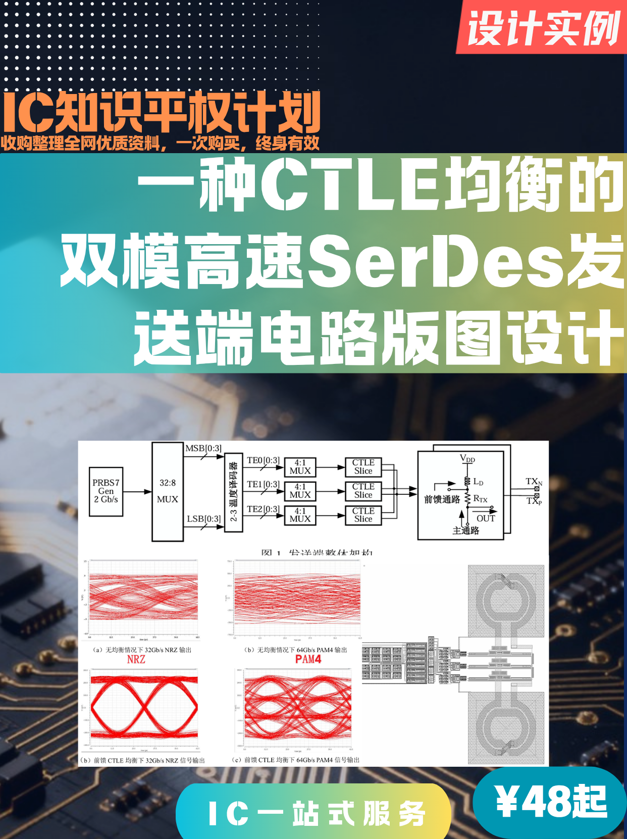
一种CTLE均衡的双模高速SerDes发送端
一种CTLE均衡的双模高速SerDes发送端
【serdes】采用Ctle的多模高速serdes发射机,电路版图文档 1、该文档描述了一种支持双模(NRZ/PAM4)的高速SerDes发送端设计,重点通过改进的CTLE均衡技术解决高损耗信道下的信号衰减问题。 2、该设计通过模块化架构(树形MUX、温度译码器、高精度时钟)和创新的CTLE前馈通路,实现了32/64 Gb/s双模高速传输。 3、改进的CTLE均衡技术显著提升了高频信号补偿能力,仿真结果验证了其在NRZ和PAM4模式下的可靠性和信号完整性,适用于高损耗信道场景。 版图不完整,主要是出电路+设计文档。设计文档5页,参考文献英文3篇。工艺28nm
完整版私信客服 186-6709-0885
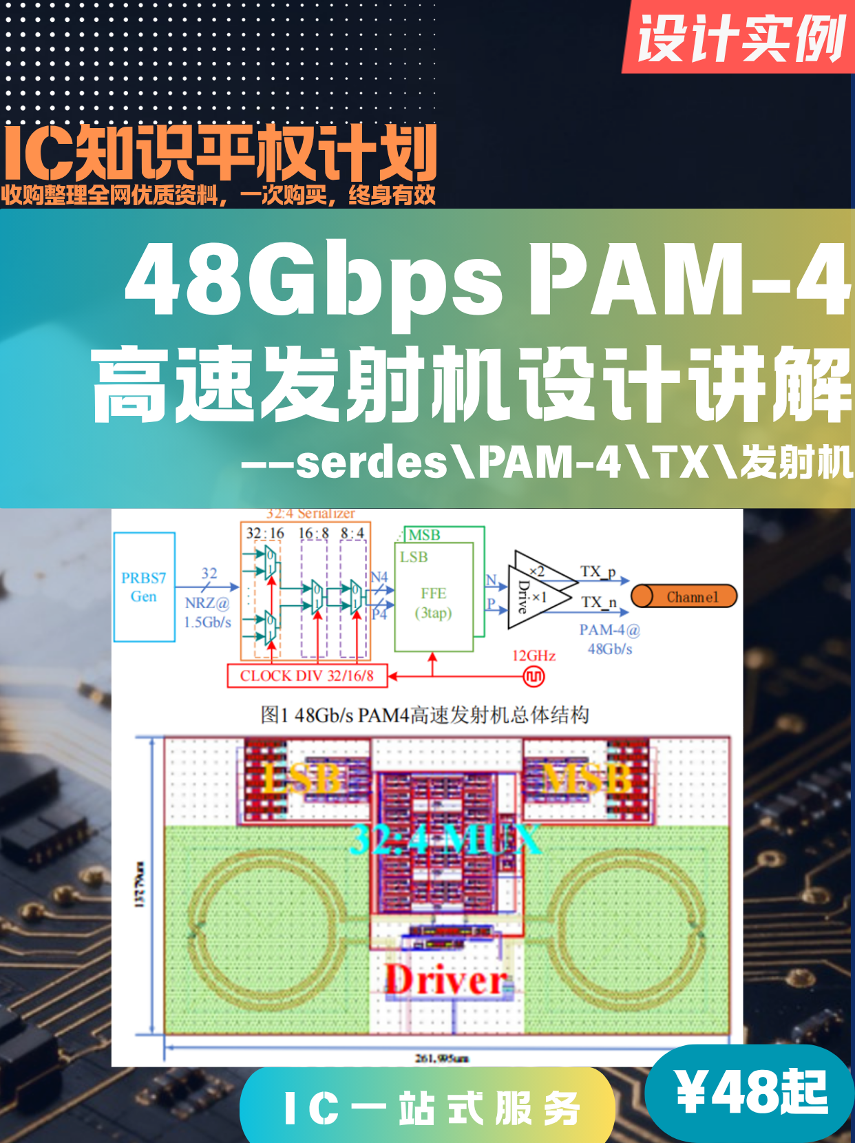
48Gb/s PAM4高速发射机电路版图设计
48Gb/s PAM4高速发射机电路版图设计
[SerDes]48Gb/s PAM4高速发射机 发货内容: 1、电路版图文件+PDK 2、15页中文电路原理和仿真结果介绍、改进计划、verilogA等内容 包括了32:4多路复用器(MUX)、 双路半速率3-tap FFE和输出组合驱动器。伪随机数产生模块(PRBS7)产生32 路1.5Gb/s并行数据流,经32:4 MUX后产生差分的4路12Gb/s NRZ数据,分别传 输至MSB和LSB延时路径块中经过延迟和速率合成,最后将产生的两路24Gb/s NRZ信号通过组合驱动器合为一路48Gb/s PAM-4信号,并送入信道中。 serdes\cedence\PAM-4\TX\发射机
完整版私信客服 186-6709-0885
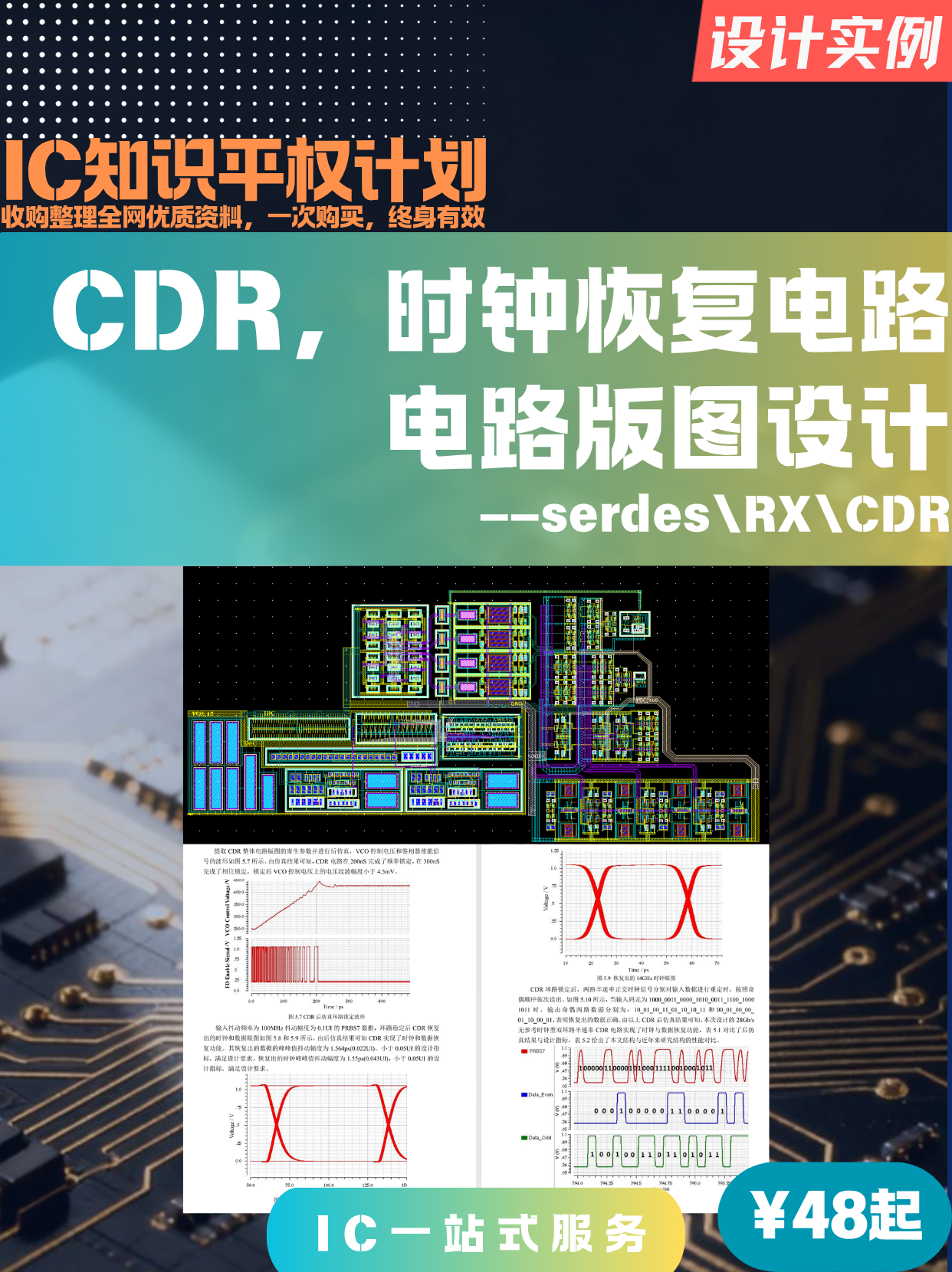
CDR时钟恢复电路版图设计
CDR时钟恢复电路版图设计
SerDes接收机CDR,时钟恢复电路 1、发货内容:电路版图PDK+配套PDF文档(50页建模+电路+版图+仿真)+参考资料 时钟数据恢复(CDR)电路作为SerDes接收机中的核心电路,负责从接收到具有抖动的串行数据流中恢复出低抖动的时钟信号,并对数据进行重定时恢复出眼图清晰的数据信号,送入后续串并转换电路进行处理。 本文采用UMC_28nmCMOS工艺设计了一种基于PLL型28Gb/sSerDes系统的双环路半速率结构CDR, 主要包括:伪差分环形振荡器(PDRO)、半速率Bang-Bang鉴相器(BBPD)、全速率鉴频器(FD)、电荷泵(CP)、电压-电流(V-I)转换器以及延时单元等关键电路模块。 本文从电路结构、模型建立、电路设计和版图布局等层面对CDR电路进行了深入研究,主要内容如下: (1)对不同结构的CDR电路在抖动特性、环路稳定性、功耗、建立时间以及电路复杂度等方面进行对比分析,采用基于PLL型的双环路半速率结构CDR作为本设计的拓扑结构,并提出一种频率检测电路能够实现在频率锁定后自动切断频率锁定环路; (2)针对本文采用的CDR拓扑结构,在详细分析了相位锁定环路与频率锁定环路的环路特性后,提出了CDR环路参数设计步骤; (3)基于Verilog-A 行为描述语言对CDR系统进行了行为级建模和仿真验证,并基于行为级模型完成了环路参数的优化; (4)采用28nmCMOS工艺完成CDR电路和版图设计并进行后仿真验证工作。 28Gb/s SerDes CDR 电路整体版图面积为160μm×80μm,版图后仿真结果表明:在TT 工艺下,输入28Gb/s的PRBS7数据,CDR恢复出的时钟和数据的峰峰值抖动幅度分别为1.55ps(0.043UI)和 1.564ps(0.022UI),在 1.05V 电源电压下测得系统总功耗为21mW。本文设计的28Gb/sCDR电路功能正确,恢复出的时钟和数据的峰峰值抖动性能以及系统功耗均达到预期设计指标。 关键字:高速串行接口;时钟数据恢复;环形振荡器;半速率Bang-Bang鉴相器;抖动
完整版私信客服 186-6709-0885
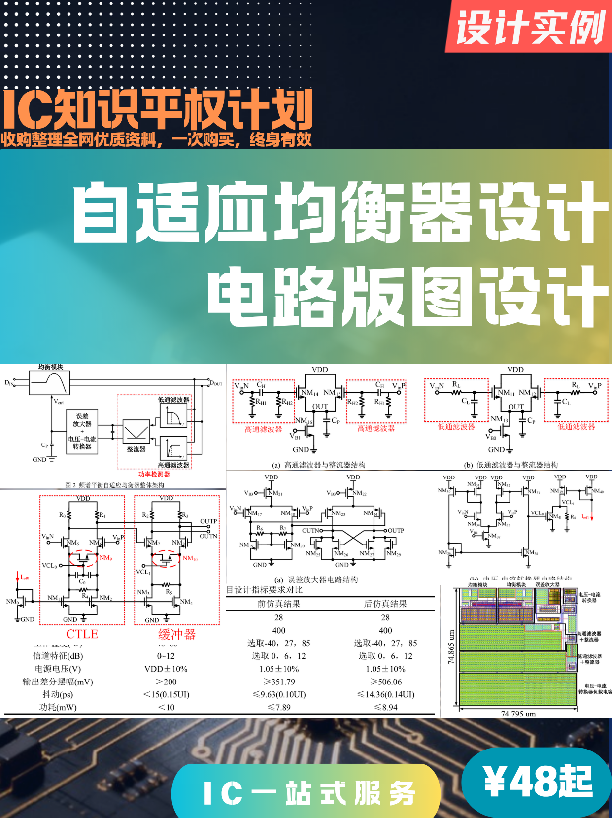
自适应均衡器电路版图设计讲解
自适应均衡器电路版图设计讲解
自适应均衡器设计,电路版图PDK+视频讲解+配套文档 A、发货内容: 电路版图PDK。13页配套文档+多篇参考文献。10分钟视频讲解原理和仿真 B、特色: 1. 先进的设计工艺:采用UMC 28nm CMOS工艺,符合当前半导体行业对高性能、低功耗的追求,有助于提升产品在市场上的技术先进性。 2. 自适应均衡技术:设计采用了频谱平衡自适应方法,能够实时跟踪信道变化,提高通信系统的性能和可靠性,满足高速数据传输的需求。 3. 模块化设计:均衡器由多个模块组成,包括CTLE、功率检测器、误差放大器和电压-电流转换器等,这种模块化设计便于维护和升级,增强了产品的灵活性和可扩展性。 4. 性能指标优异:前仿真和后仿真结果均显示,设计满足了严格的性能指标,如输出差分摆幅、抖动和功耗等,这些指标对于通信设备的性能至关重要。 5. 版图设计优化:版图面积仅为0.0056mm²,这有助于降低生产成本,同时保持高性能,对于追求成本效益的客户来说具有吸引力。 6. 广泛的仿真条件:设计在不同的工作温度、电源电压和信道损耗条件下进行了仿真,确保了产品的稳定性和可靠性,这对于在不同环境条件下使用的通信设备尤为重要。 7. 详细的仿真结果:报告提供了详细的前仿真和后仿真结果,包括眼图、抖动、功耗等关键参数,这些数据为产品的性能验证提供了有力支持。 8. 满足设计指标:所有设计指标均满足题目要求,这表明设计不仅在理论上可行,而且在实际应用中也具有良好的性能表现。
完整版私信客服 186-6709-0885
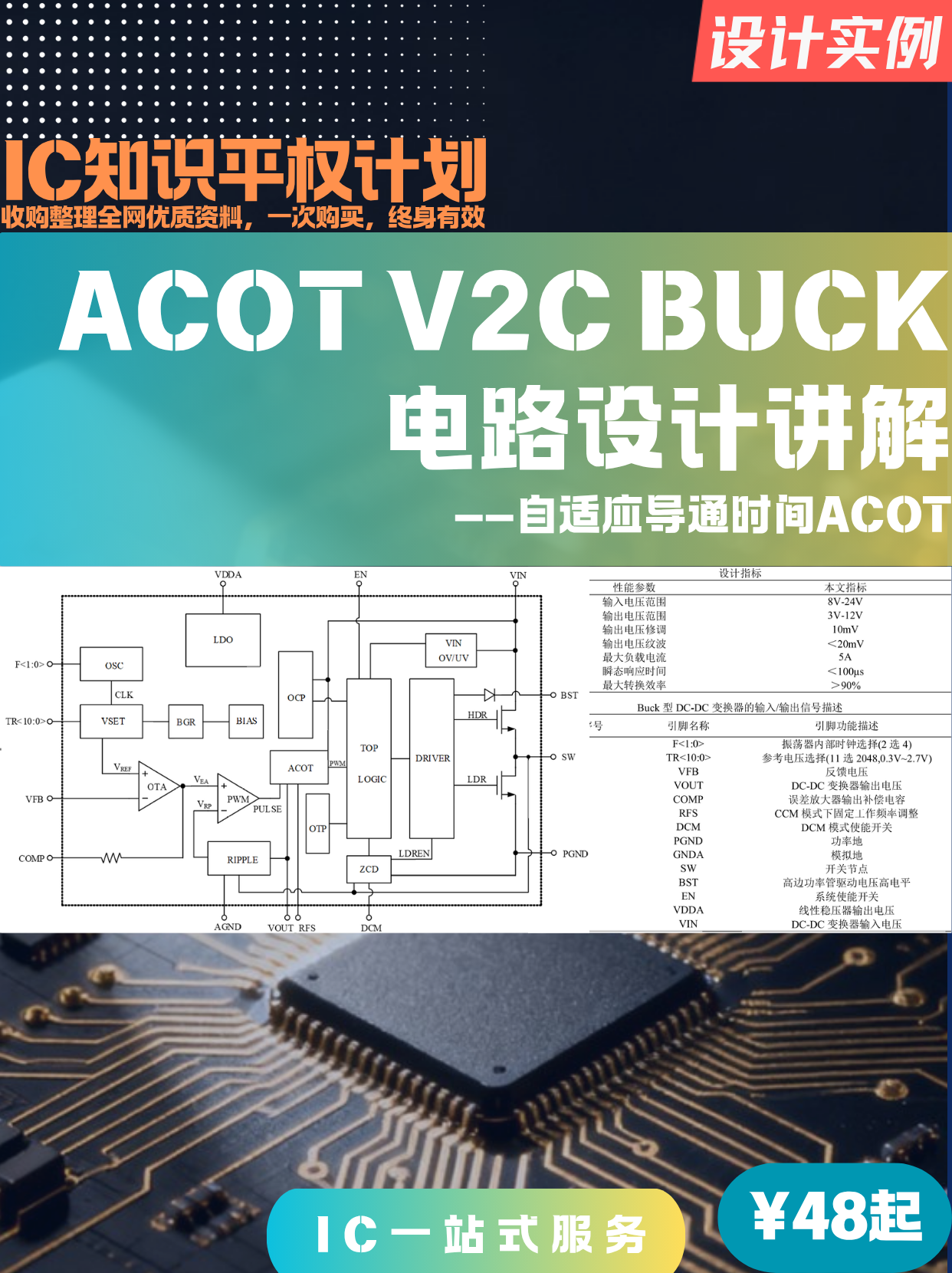
ACOT V2C BUCK电路设计讲解
ACOT V2C BUCK电路设计讲解
ACOT V2C BUCK电路】 发货内容: 1、完整BUCK电路-TOP-DOWN,+PDK(BCD工艺) 2、30页PDF文档,1W字以上分析(理论分析,电路介绍,部分仿真结果) 3、简要视频概述 性能 输入最高24V电压,最大5A负载电流(可拓展),输出电压可修调,软启,DCM/FCCM切换,自适应Ton可修调,最小toff时间,纹波补偿,各类保护电路。
完整版私信客服 186-6709-0885
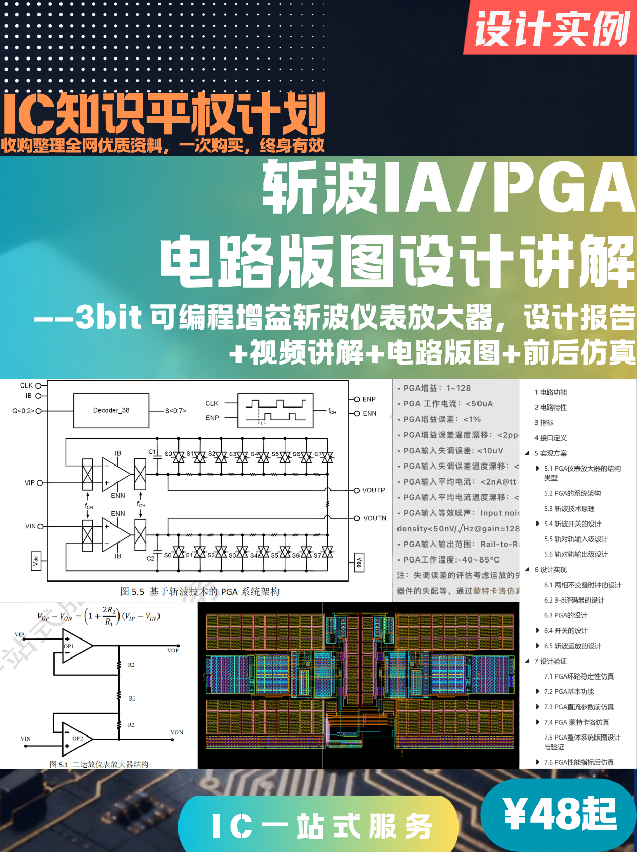
斩波PGA/IA电路版图设计讲解
斩波PGA/IA电路版图设计讲解
斩波仪表放大器IA/可编程增益放大器PGA 电路版图设计讲解 3bit 可编程增益斩波仪表放大器(Chopper Instrumentation PGA) 发货内容: 1、PDF设计文档60页-原理分析+电路设计+仿真解析 2、讲解视频60分钟 3、电路版图文件 特点:采用仪表放大器形式(常见的为双运放结构);电阻阵列采用抽头式并由数字码控制增益的切换;运放结构为经典的RTR输入输出结构,同时采用动态失调噪声降低技术,例如斩波自零等。 电路版图均已完成,仿真结果如下图。已实现轨到轨输入输出,最大5uV失调,47uA功耗,19nV低噪声等核心指标。
完整版私信客服 186-6709-0885
【电路之美-拉扎维-11】数字模拟转换器(DAC)与电机驱动电路设计
【电路之美-拉扎维-11】数字模拟转换器(DAC)与电机驱动电路设计
视频标题 《电路之美》系列:数字模拟转换器(DAC)与电机驱动电路设计 --- 视频简介 本视频由扎德·拉扎维(Behzad Razavi)教授主讲,深入探讨机器人系统中数字控制器与模拟电机驱动之间的接口设计问题。课程从机器人手臂抓取鸡蛋的实际应用出发,逐步讲解: - 为何需要数字-模拟转换器(DAC)作为桥梁 - 二进制加权电流源型DAC的工作原理(2位及3位示例) - 使用MOSFET实现电流源与开关的具体电路方案 - 电流镜技术在精确复制电流中的应用 - 关键设计挑战:电机感性负载导致的电压尖峰问题及其解决方案——续流二极管保护电路 本集完美诠释了理论分析与工程实践的结合,展现了模拟电路设计中的"美学"思维。 --- 关键词 数字模拟转换器、DAC、二进制加权电流源、电流镜\MOSFET、电流源、模拟开关、续流二极管\电机驱动、机器人控制、感性负载保护电感电压尖峰、开关瞬态、电路保护设计\拉扎维、电路之美、模拟集成电路设计 |
完整版私信客服 186-6709-0885
[SerDes]CDR带宽为何如此重要?——从眼图抖动跟踪到高速串行通信设计
[SerDes]CDR带宽为何如此重要?——从眼图抖动跟踪到高速串行通信设计
视频标题 CDR带宽为何如此重要?——从眼图抖动跟踪到高速串行通信设计 --- 视频简介 本视频深入解析时钟数据恢复(CDR)电路中的核心参数——环路带宽。通过"汽车转向"的生动类比,揭示CDR带宽的本质:它决定了接收机跟踪数据眼图移动的速度能力。 视频系统阐述了两大关键问题: - 必须跟踪的时序变化:低频时钟漂移、PPM频偏、扩频时钟(SSC)、电源噪声等 - 必须抑制的高频干扰:随机噪声、高频抖动、串扰、ISI引起的边沿偏移 详细讲解高CDR带宽带来的七大优势:改善低频抖动容限、提升PPM容差、确保SSC跟踪、避免斜率过载、抑制本地振荡器噪声、缩短锁定时间、增强突发模式捕获。同时介绍"齿轮切换"自适应带宽等实用设计技巧,并列举带宽不足的典型故障征兆。 适合高速SerDes设计工程师、信号完整性工程师及学习高速接口技术的电子工程专业学生观看。 --- 关键词 ``` CDR, 时钟数据恢复, CDR带宽, 抖动容限, Jitter Tolerance, 扩频时钟, SSC, PPM频偏, 眼图, 高速串行通信, SerDes, Bang-Bang CDR, 斜率过载, 环路带宽, 相位噪声, 锁定时间, 自适应带宽, 齿轮切换, 信号完整性, 高速接口, PCIe, USB
完整版私信客服 186-6709-0885
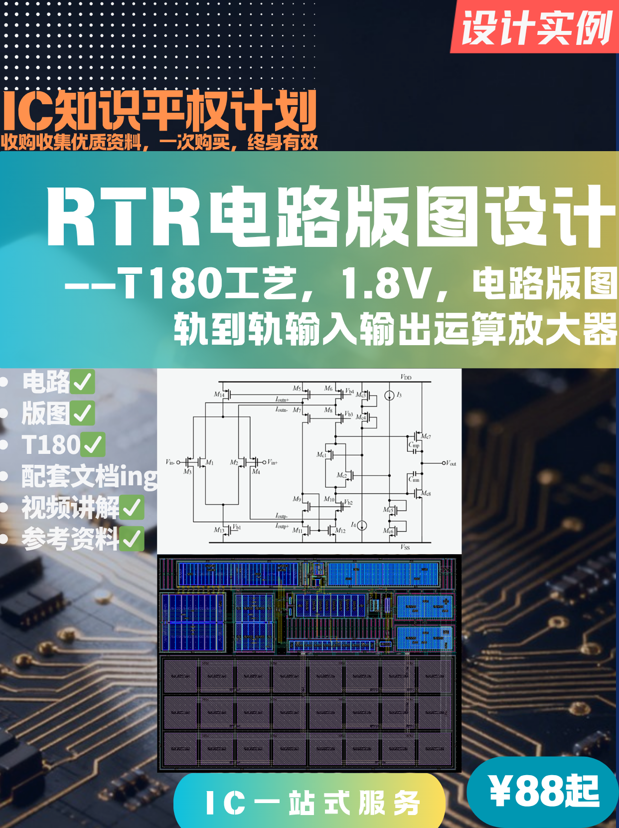
RTR电路版图设计讲解
RTR电路版图设计讲解
轨到轨运放RTR电路版图设计讲解 轨对轨(功率)运算放大器。 1.大厂T180工艺,100%输入电压范围,100%输出电压范围,开环直流增益>100dB,电源抑制比>90dB。 2.P/N共同输入,class ab级输出。 3.仿真testbench包含:IQ仿真/STB稳定性仿真/CMRR仿真/PSRR仿真/输入共模范围仿真/输出共模范围仿真/建立时间仿真/SR仿真 4.资料包含相关设计资料+电路原理图+版图(过DRC/LVS)+Testbench(上述提到)+部分仿真结果 注:本链接只包含上述内容,如需额外拓展/设计辅导/版图辅导/工具使用技巧,请私聊询价,谢谢!
完整版私信客服 186-6709-0885
![[SerDes]TIA跨阻放大器:光学接收器的核心,为何在电学链路中未必适用?](https://material-image.wanwang.xin/1597234105050516/public/2232e1de-ed50-4bf7-8b3a-29d778885b57.png)
[SerDes]TIA跨阻放大器:光学接收器的核心,为何在电学链路中未必适用?
[SerDes]TIA跨阻放大器:光学接收器的核心,为何在电学链路中未必适用?
跨阻放大器(TIA, Transimpedance Amplifier)是光学通信接收器的标准配置,它将光电二极管的电流信号转换为电压信号。但在高速电学链路(如PAM4、Chiplet互连)中,TIA的应用场景却大不相同。 本视频深入解析: - 光学TIA的核心挑战:高增益、宽带宽、低噪声的三难权衡 - 电学链路的本质差异:传输线匹配 vs 电流源驱动 - 电学接收器中TIA的真实位置:内部GM-CTLE后的有源增益级 - 电流模式感知的优势与代价:噪声、稳定性、校准复杂度 - 何时该用、何时不该用:从CPO/光学IO到超短距Chiplet链路的选型判断
完整版私信客服 186-6709-0885
[SerDes]TIA跨阻放大器:光学接收器的核心,为何在电学链路中未必适用?
[SerDes]TIA跨阻放大器:光学接收器的核心,为何在电学链路中未必适用?
视频标题 TIA跨阻放大器:光学接收器的核心,为何在电学链路中未必适用? 视频简介 跨阻放大器(TIA, Transimpedance Amplifier)是光学通信接收器的标准配置,它将光电二极管的电流信号转换为电压信号。但在高速电学链路(如PAM4、Chiplet互连)中,TIA的应用场景却大不相同。 本视频深入解析: - 光学TIA的核心挑战:高增益、宽带宽、低噪声的三难权衡 - 电学链路的本质差异:传输线匹配 vs 电流源驱动 - 电学接收器中TIA的真实位置:内部GM-CTLE后的有源增益级 - 电流模式感知的优势与代价:噪声、稳定性、校准复杂度 - 何时该用、何时不该用:从CPO/光学IO到超短距Chiplet链路的选型判断 适合高速模拟IC设计工程师、光通信/电通信系统架构师,以及想了解接收机前端设计 trade-off 的读者。 关键词 跨阻放大器,TIA,Transimpedance Amplifier,光学接收器,光电二极管,PAM4接收机,高速SerDes,电流模式,电压模式,CTLE,连续时间线性均衡器,GM-CMOS,传输线匹配,输入阻抗,带宽增益积,输入参考噪声,CPO,共封装光学,Chiplet互连,模拟前端,AFE,高速链路设计
完整版私信客服 186-6709-0885
![[TI]《自适应导通时间控制(ACOT)深入研究》](https://material-image.wanwang.xin/1597234105050516/public/bcbed098-8312-447c-8782-1a4e193e177d.png)
[TI]《自适应导通时间控制(ACOT)深入研究》
[TI]《自适应导通时间控制(ACOT)深入研究》
本期视频由德州仪器应用工程经理Tahar Alag主讲,深入讲解开关电源中常见的控制拓扑架构,包括固定频率控制模式(电压模式控制、电流模式控制)、自适应导通时间控制(COT)的基本原理、优势与局限性,以及D-CAP系列架构(D-CAP、D-CAP2、D-CAP3、D-CAP4)的演进,并提供控制模式选型对比表,适合电源设计工程师、硬件工程师及电子工程专业学生学习参考。
完整版私信客服 186-6709-0885
CPO-intel-共封装光学(CPO)规模化——突破AI时代的I/O瓶颈
CPO-intel-共封装光学(CPO)规模化——突破AI时代的I/O瓶颈
本视频为英特尔晶圆代工(Intel Foundry)关键人物Nick Sila在2024年政府会议上的主题演讲实录。作为Optoscribe被收购后加入英特尔的核心技术专家,Sila深入剖析了人工智能计算面临的根本性挑战——内存带宽与I/O带宽无法跟上算力增长的"内存墙"问题。 演讲核心内容包括: - AI扩展的瓶颈:为什么I/O密度和能效成为制约AI系统规模化的关键因素 - CPO与先进封装:共封装光学如何与铜缆互补,实现从短距到长距的高带宽、低功耗连接 - 制造转型挑战:将光子学从手工组装转向晶圆级、大批量电子制造流程的必要性 - 玻璃芯基板(Glass Core):英特尔最新展示的24层玻璃芯基板技术,为超高密度光互连提供可扩展平台 - 未来愿景:从芯片级到面板级的全光连接矩阵,构建下一代AI系统的技术路线图 Sila特别强调,CPO的成功需要整个生态系统的巨额投资,涵盖从组件供应、测试设备到封装能力的全产业链准备,以应对未来百万级光链路数据中心的爆发式需求。
完整版私信客服 186-6709-0885
【电路之美-拉扎维-10】从机器人到运放
【电路之美-拉扎维-10】从机器人到运放
视频标题 《电路之美:机器人如何温柔地拿起一颗鸡蛋——从惠斯通电桥到精密控制》 --- 视频简介 在本期《电路之美》系列中,贝扎德·拉扎维教授以机器人抓取鸡蛋这一经典工程挑战为切入点,深入浅出地讲解了精密压力检测电路的设计原理。 从最简单的电阻分压电路出发,视频逐步揭示了为什么直接测量微小电压变化困难重重,并引出惠斯通电桥这一巧妙结构——通过差分测量将淹没在大直流信号中的微小变化转化为易于检测的零基信号。更进一步,教授展示了如何利用双传感器配置使灵敏度翻倍,以及运算放大器如何构建闭环控制系统,让机械臂"感知"压力并精准停止。 最后,视频将电路原理与动态响应特性相联系,通过过阻尼、欠阻尼和临界阻尼的直观对比,说明工程设计中速度与稳定性的权衡艺术——太快会捏碎鸡蛋,太慢则效率低下,而优秀的工程师懂得在两者之间寻找最优解。 这是一堂将传感器技术、模拟电路与控制系统融会贯通的精彩课程。 --- 关键词 惠斯通电桥、电阻式压力传感器、差分放大、运算放大器、闭环控制\电阻分压、灵敏度提升、共模抑制、非反相放大器、基准电压比较\机器人触觉、力控制、机械臂、自动化抓取、柔性制造\过阻尼、欠阻尼、临界阻尼、系统响应、稳定性分析\电路之美、模拟集成电路、传感器接口、贝扎德·拉扎维 |
完整版私信客服 186-6709-0885
[SerDes]CTLE设计陷阱:为什么增益够了,眼图却变差了?——群时延与相位的重要性
[SerDes]CTLE设计陷阱:为什么增益够了,眼图却变差了?——群时延与相位的重要性
本视频深入解析高速串行通信中CTLE设计的常见误区,重点探讨工程师只关注增益提升而忽略相位响应和群时延特性的问题,包括CTLE增益提升后眼宽恶化的原因、群时延的物理意义及对信号完整性的影响、PAM4调制中的眼图偏移问题、过度峰化带来的过冲陷阱,以及三种实用的群时延优化方案和后端自适应均衡中的时域感知机制,适用于25G/56G/112G SerDes设计工程师及关注高速信号完整性的硬件开发者。
完整版私信客服 186-6709-0885
【电路之美-拉扎维-09】电动汽车逆变器原理:从电池直流到电机交流的电路实现
【电路之美-拉扎维-09】电动汽车逆变器原理:从电池直流到电机交流的电路实现
本视频由Behzad Razavi教授讲解电动汽车动力系统的核心部件——功率逆变器。视频从电动汽车的基本架构出发,解释了为何需要将电池的直流电转换为交流电来驱动电机。通过逐步构建电路模型,演示了如何利用四个开关器件(MOSFET)交替导通,产生正负交替的交流输出波形。进一步分析了实际应用中的关键挑战:大电流(40A)下的导通损耗问题,以及高电压(600V)下的器件耐压要求。最后介绍了现代功率半导体器件(如Infineon的750V/60mΩ MOSFET)如何满足这些苛刻指标,实现高效、可靠的电能转换。
完整版私信客服 186-6709-0885
半导体器件物理-14.从平面MOSFET到FinFET、GAA与CFET的演进之路
半导体器件物理-14.从平面MOSFET到FinFET、GAA与CFET的演进之路
这是一门讲解先进半导体晶体管技术演进的课程内容,围绕半导体器件物理展开,梳理从平面MOSFET到FinFET、GAA、CFET的技术发展路径,分析平面MOSFET在28nm以下节点面临的各类核心物理挑战,详解三类新型晶体管架构的特点、原理、优势与制造难点,结合英特尔、台积电、三星等厂商的技术路线,拆解22nm到2nm节点的产业发展脉络,还展望了二维材料相关的未来技术方向,适配微电子、集成电路相关领域的学生与工程师学习。
完整版私信客服 186-6709-0885
Intel Computex 2026 主题演讲|CEO陈立武宣布18A制程全面量产,揭晓Xeon 6+、Agentic AI与异构计算未来蓝图
Intel Computex 2026 主题演讲|CEO陈立武宣布18A制程全面量产,揭晓Xeon 6+、Agentic AI与异构计算未来蓝图
Intel首席执行官陈立武(Lip-Bu Tan)在2026年台北国际电脑展(Computex)发表年度主题演讲,全面展示Intel转型一年的核心成果与未来战略。本次演讲重点包括18A制程全面量产、数据中心革新、AI生态布局、定制芯片业务及边缘与物理AI等方面,强调Intel正从"传统IDM"向"以工程为核心、以生态为驱动"的新模式加速转型,通过开放标准与异构计算,重新定义AI时代的计算基础设施。
完整版私信客服 186-6709-0885
![[曲博]深度解读华为韬定律:从晶体管密度到时间常数τ,如何用“时间缩微”重定义芯片未来](https://material-image.wanwang.xin/1597234105050516/public/8eccb8e2-d3b7-458a-8128-f9d417642f47.png)
[曲博]深度解读华为韬定律:从晶体管密度到时间常数τ,如何用“时间缩微”重定义芯片未来
[曲博]深度解读华为韬定律:从晶体管密度到时间常数τ,如何用“时间缩微”重定义芯片未来
摩尔定律正在逼近物理极限,单纯靠缩小晶体管已难以为继。2026年,华为正式提出“韬(τ)定律”,将半导体演进的评判核心从晶体管密度转向信号传播时间常数τ,并推出核心落地技术——逻辑折叠(Logic Folding)。 本期视频系统拆解韬定律的四层时间常数体系(晶体管层→电路层→芯片层→系统层),详解逻辑折叠如何通过细粒度3D立体设计,在固定工艺节点下实现芯片面积缩小40%、时脉提升37%、功耗降低24%的显著收益。 华为披露,基于韬定律已量产381款芯片,覆盖手机、AI、汽车等多领域。2026年麒麟芯片将首次商用逻辑折叠,混合键合间距达1.5微米,领先台积电与Intel同期方案。 同时,我们也会讨论韬定律面临的争议:等效晶体管密度的计算方式是否合理?EDA工具链、散热等挑战如何解决?以及这一范式转换对中国半导体产业的战略意义。 如果你关心芯片后摩尔时代的破局之路,这期视频不容错过。
完整版私信客服 186-6709-0885
[CPO]2026 CPO 技术论坛|从电到光的关键转折:先进封装测试挑战与 Hyper Socket 解决方案全解析
[CPO]2026 CPO 技术论坛|从电到光的关键转折:先进封装测试挑战与 Hyper Socket 解决方案全解析
2026 CPO技术论坛由颖微科技举办,该公司将2026年定义为“CPO元年”。论坛中,执行副总陈绍坤开启序幕,技术行销处长孙家斌博士梳理了CPO从产业并购潮、光学引擎(OE)设计到先进封装测试瓶颈的完整脉络,涵盖电与光物理特性差异、光学引擎位置对CPO的定义、光学路径挑战、单模光纤对准公差量产困境等内容,并介绍了颖微科技针对各阶段提出的测试界面方案,最后Q&A环节直击核心问题,适合半导体投资者、封装测试产业人士与先进制程研究者参考。
完整版私信客服 186-6709-0885
NVIDIA Vera:专为智能体时代打造的CPU | 从"演奏者"到"指挥家"的架构革命
NVIDIA Vera:专为智能体时代打造的CPU | 从"演奏者"到"指挥家"的架构革命
当AI智能体成为主流,传统CPU架构正面临根本性挑战。本视频深度解析NVIDIA全新发布的Vera CPU——首款专为"智能体循环"设计的数据中心处理器。我们将揭秘Vera如何通过三大创新重塑计算架构:Olympus核心、LPDDR5X内存系统、第二代可扩展一致性互联。从NVLink芯片直连到BlueField 4 STX智能网卡集成,看Vera如何与Rubin GPU协同,将CPU从GPU的"瓶颈"转变为AI工厂的"指挥中枢",实现1.8倍于x86的智能体沙箱性能。
完整版私信客服 186-6709-0885
[量子计算×英伟达]Ising AI模型如何破解最大难题
[量子计算×英伟达]Ising AI模型如何破解最大难题
2026年4月14日,英伟达CEO黄仁勋发布全球首个专为量子计算设计的开源AI模型套件Ising。量子计算机虽被视为下一代算力终极形态,但量子比特易受外界影响而“坍缩”成噪音,传统算法纠错速度慢。Ising通过预测错误,借助英伟达相关GPU算力,将量子纠错速度提升2.5倍、精度提高3倍,大幅缩短量子系统校准时间。英伟达不造量子芯片,旨在通过开源Ising复制CUDA成功路径,成为所有量子计算机的“大脑”,构建AI与量子加速进化的技术闭环。
完整版私信客服 186-6709-0885
[SerDes]边缘DFE/CDR深度解析
[SerDes]边缘DFE/CDR深度解析
在高速串行通信系统中,多数人关注数据DFE以打开数据眼图,却忽略边缘采样点的码间干扰(ISI)。本视频深入解析CDR接收机核心机制,指出当数据眼图干净但边缘交叉点存在ISI时,恢复的时钟会产生噪声,导致“坏边缘→坏时钟→更差数据采样”的恶性循环,此问题仅靠数据DFE无法解决。视频重点介绍边缘ISI导致的问题、传统方法的局限,以及Type-2 XDFE架构、改进型LMS算法等解决方案,并通过实测验证其效果,强调对于56G/112G等现代高速链路,边缘DFE已成为必需技术。
完整版私信客服 186-6709-0885
电路之美-拉扎维-8:用光电二极管测量心率与血压的奥秘
电路之美-拉扎维-8:用光电二极管测量心率与血压的奥秘
《电路之美:用光电二极管测量心率与血压的奥秘》 视频简介 本视频由著名电路设计专家Behzad Razavi教授主讲,深入讲解如何利用简单的电路元件实现人体关键生命体征——心率和血压的测量。视频从人体血液循环的基本原理出发,逐步剖析光电容积脉搏波描记法(PPG)的工作机制:通过LED向手指发射光线,利用光电二极管检测透射光强度的周期性变化,从而捕捉心脏收缩与舒张引起的血容量波动。Razavi教授详细解释了光电二极管将光信号转换为电流的物理过程,并进一步介绍了基于积分电容、复位开关和源极跟随器的信号处理电路设计。最后展示了实际测量得到的心率波形(83次/分钟),完整呈现从物理原理到电路实现的工程美学。 关键词 光电二极管、LED、积分电容、源极跟随器、心率测量、血压监测、脉搏波、光电容积脉搏波(PPG)、跨阻放大、电流积分、开关电容电路、模数转换、可穿戴设备、医疗电子、生物传感、生命体征监测、耗尽区、电子-空穴对、反向偏置、采样频率 |
完整版私信客服 186-6709-0885
[SerDes]CTLE、TX-FIR与DFE协同工作原理
[SerDes]CTLE、TX-FIR与DFE协同工作原理
本视频通过交互式仿真工具,直观演示高速串行链路中的关键均衡技术。从基础的TX-FIR预加重、CTLE连续时间线性均衡,到DFE判决反馈均衡器,逐步展示如何"打开"闭合的眼图。适合信号完整性工程师、高速电路设计人员及相关专业学生学习参考。
完整版私信客服 186-6709-0885
[SerDes]为什么接收端(RX) FFE必须使用采样保持放大器?——高速SerDes模拟均衡器设计深度解析
[SerDes]为什么接收端(RX) FFE必须使用采样保持放大器?——高速SerDes模拟均衡器设计深度解析
本视频深入解析56G PAM4高速串行通信接收机中前馈均衡器(FFE)的核心设计挑战,探讨为何接收端(RX) FFE必须采用采样保持(S/H)放大器架构,而发送端(TX) FFE可用简单数字移位寄存器实现,并从架构差异、实现难点及创新方案三个关键维度展开分析,同时探讨不能单纯依赖TX FFE而取消RX FFE的原因,适合高速SerDes设计工程师、模拟/混合信号IC设计人员及相关专业研究生参考。
完整版私信客服 186-6709-0885
![[TI]EIS电化学阻抗谱技术解析与TI解决方案](https://material-image.wanwang.xin/1597234105050516/public/f6f0996c-9a3d-45fe-b503-36849654f81c.png)
[TI]EIS电化学阻抗谱技术解析与TI解决方案
[TI]EIS电化学阻抗谱技术解析与TI解决方案
大纲 传统BMS的性能鸿沟 EIS电化学阻抗谱原理揭秘 EIS带来的三大核心优势 TI EIS解决方案与芯片架构 实战测试与精准度验证 结束 总结与展望
完整版私信客服 186-6709-0885
[封装]CoPos介绍
[封装]CoPos介绍
台积电CoPoS技术深度解析:方形玻璃载板如何颠覆先进封装?破解媒体三大误解 视频简介 台积电董事长魏哲家在2024年4月法说会上宣布「CoPoS将取代CoWoS」,瞬间引爆科技媒体热议。然而,几乎所有媒体的解读都是错的! 本视频由台积电董事长魏哲家亲自讲解,彻底厘清三大常见误解: - ❌ 误解:CoPoS是用方形玻璃面板取代圆形硅晶圆作为中介层 - ❌ 误解:CoPoS是用玻璃中介层取代硅中介层 - ✅ 真相:CoPoS核心创新是用方形玻璃临时载板取代圆形玻璃临时载板,大幅提升面积利用率、降低成本 视频完整解析台积电先进封装技术版图: - 从WLCSP晶圆级封装到FOWLP/FOPLP扇出型封装 - 从CoWoS-S/CoWoS-L/CoWoS-R到CoPoS的技术演进 - 芯片分割(Chiplet)如何提升良率、降低成本 - 3D封装、HBM高带宽内存、系统整合芯片(SoIC)完整架构 - 未来AI/HPC平台:光电共封装(Co-Packaged Optics)前瞻布局 无论你是半导体从业者、投资人或科技爱好者,这堂课将帮你建立最准确的先进封装知识框架,不再被错误信息误导! 关键词 CoPoS、CoWoS、先进封装、晶圆级封装、扇出型封装、FOWLP、FOPLP、3D封装、2.5D封装、芯片分割、Chiplet、HBM、高带宽内存、硅中介层、玻璃中介层、临时载板、TSV、微凸块、SoIC、InFO、CoWoS-S、CoWoS-L、CoWoS-R、WMCM、系统整合芯片、整合式扇出型封装、AI芯片、高性能运算、HPC、数据中心、手机处理器、A20 Pro、光电共封装、CPO、台积电、魏哲家、TSMC、半导体制造、摩尔定律、圆形玻璃vs方形玻璃、硅中介层vs玻璃中介层、晶圆级vs面板级、SoC vs Chiplet
完整版私信客服 186-6709-0885
[SerDes]56Gbps PAM4接收器CTLE设计实战
[SerDes]56Gbps PAM4接收器CTLE设计实战
本视频为ICONS 2026"高级IC设计大师课"系列第五讲,聚焦高速SerDes前端设计中的核心模块——连续时间线性均衡器(CTLE)的引导式设计全流程。针对56 Gbps PAM4面板接收机通过8 dB损耗信道的典型应用场景,系统讲解如何运用一阶方程进行手算估算,并逐步确定关键设计参数,还将展示Cadence瞬态仿真结果,对比CTLE前后眼图的开启度变化,帮助学习者建立从理论估算到晶体管级验证的完整设计直觉。适合具备模拟IC基础、希望深入高速接口电路设计的工程师与研究生。
完整版私信客服 186-6709-0885
【电路之美-拉扎维-07】从手表到震荡器
【电路之美-拉扎维-07】从手表到震荡器
视频标题 《晶体振荡器:手表如何精确计时?——拉扎维电路设计精讲》 --- 视频简介 本集由著名模拟电路专家贝赫扎德·拉扎维(Behzad Razavi)主讲,深入解析石英手表背后的电路原理。从1Hz时间基准的生成出发,讲解如何通过级联计数器实现秒、分、时的精确计数;重点剖析晶体振荡器的高精度与低功耗特性,并揭示一个关键工程挑战——为何手表中的33kHz晶体必须通过15位分频器才能产生1秒脉冲。最后通过CMOS反相器与晶体的极简电路设计,展示如何实现每月误差仅1秒的高精度振荡。适合电子工程学生、硬件工程师及钟表技术爱好者学习。 --- 关键词 晶体振荡器、石英手表、1Hz时间基准、15位计数器、CMOS反相器、压电晶体、频率分频、低功耗设计、精密计时、模拟电路、拉扎维、电路设计、振荡器原理、电子表芯、33kHz晶振
完整版私信客服 186-6709-0885
[SerDes]56G高速SerDes接收机创新架构:单时钟动态采样级实现回声消除、串扰抵消与高频均衡
[SerDes]56G高速SerDes接收机创新架构:单时钟动态采样级实现回声消除、串扰抵消与高频均衡
本视频深入解析高速串行通信接收机面临的核心挑战:传统模拟均衡器(CTLE、FFE、DFE)在功耗、速度与复杂度上的三重困境。重点介绍一种革命性的时钟控制动态采样级架构,该设计在单一采样窗口内同时完成回声消除、近端串扰抵消和插入损耗均衡三大功能。适用于56Gbps及以上高速SerDes、光通信收发器及低功耗多通道接口设计。
完整版私信客服 186-6709-0885
【电路之美-拉扎维-06】从交通灯到LCVCO
【电路之美-拉扎维-06】从交通灯到LCVCO
视频标题 《交通信号灯如何检测车辆?——电感式传感器与LC振荡器原理》 --- 视频简介 本视频由著名电路设计专家毕查德·拉扎维教授讲解,从生活中常见的交通信号灯切入,深入浅出地介绍电感式车辆检测技术的工作原理。 视频首先回顾电磁学基础知识,解释磁性材料如何改变电感器的磁场分布与电感值;随后详细阐述如何将电感器埋入路面,通过车辆中的铁磁材料引起电感变化;重点讲解LC谐振回路作为振荡器的核心机制,以及实际电路中能量损耗的补偿方法——利用有源电路产生负电阻,抵消寄生电阻的影响,从而维持稳定振荡。 通过测量振荡频率的变化,交通系统即可精准判断车辆存在,实现信号灯的智能控制。本视频将电路理论与实际应用完美结合,适合电子工程学习者及对智能交通系统感兴趣的观众观看。 --- 关键词 交通信号灯、车辆检测、电感传感器、LC振荡器、谐振回路、负电阻、电磁感应、智能交通、贝赫扎德·拉扎维、电路设计、振荡器原理、磁导率、有源电路
完整版私信客服 186-6709-0885
[SerDes]224Gbps高速SerDes时钟设计:正交误差校正(QEC)与占空比校正(DCC)的关键技术
[SerDes]224Gbps高速SerDes时钟设计:正交误差校正(QEC)与占空比校正(DCC)的关键技术
本视频深入探讨112Gbps及以上高速串行通信中的核心时钟设计挑战,重点分析224G PAM4传输时,正交误差和占空比失真对眼图裕量的影响,系统讲解传统CDR的局限、正交相位检测器设计要点、占空比校正与正交误差校正的工作原理、两者的耦合关系及时序、背景自适应跟踪的必要性与实现方法,并强调将时钟子系统视为自适应系统的低功耗设计思维,为相关SerDes设计提供实战指导。
完整版私信客服 186-6709-0885
【电路之美-拉扎维-05】手机USB充电中电压转换的电路原理
【电路之美-拉扎维-05】手机USB充电中电压转换的电路原理
本文以手机USB充电为例,介绍了如何将电池或充电器提供的较高电压(如2V或5V)转换为芯片所需的较低电压(如1V)。通过分析简单电阻分压器的不足,引出利用开关周期性控制结合低通滤波器实现电压转换的方法,阐述了其工作原理及优势,即通过调节开关导通时间占比来获得所需平均电压,并利用低通滤波器抑制高频成分,得到稳定的直流电压。
完整版私信客服 186-6709-0885
【电路之美-拉扎维-04】从癌症到电容
【电路之美-拉扎维-04】从癌症到电容
本文探讨了电路设计师如何通过检测血液中Vax蛋白的浓度来帮助癌症诊断。癌症肿瘤会释放Vax蛋白到血液中,导致血液介电常数变化,进而改变电容值。通过将金属微电极插入血液形成电容,测量其电容变化可检测Vax蛋白的存在,且该方法对Vax蛋白具有特异性,不受其他蛋白质干扰。
完整版私信客服 186-6709-0885
IEEE-研讨会-AI赋能射频集成电路设计:超越人类直觉的新范式
IEEE-研讨会-AI赋能射频集成电路设计:超越人类直觉的新范式
本视频为IEEE固态电路协会(SSCS)青年卓越网络研讨会特邀演讲,由普林斯顿大学Kaushik Sengupta教授主讲。其核心内容是:传统射频集成电路(RFIC)设计高度依赖工程师经验与直觉,常陷入次优设计空间。Sengupta教授团队提出颠覆性逆向设计范式,即利用生成式AI与强化学习,从目标性能规格出发,自动探索非直观的电路架构与电磁结构。关键技术突破包括电磁结构生成式AI、可控生成、端到端RFIC设计及实测验证等。设计理念是AI将人类从繁琐迭代中解放,聚焦架构创新与创造性洞察,实现“人类直觉+算法探索”的协同设计新范式。
完整版私信客服 186-6709-0885
【电路之美-拉扎维-03】从电容变化到触摸屏手指检测
【电路之美-拉扎维-03】从电容变化到触摸屏手指检测
# 标题:触摸屏工作原理:从电容变化到手指检测 ## 简介 本内容主要从电路角度解析触摸屏(以手机屏幕为例)的工作原理,重点探讨其如何通过检测电容变化来感知手指触摸。内容从简单的平行板电容器结构入手,阐述手指靠近时引发的电场线变化及电容改变,进而介绍了多种检测电容变化的方法,包括振荡器频率变化法、恒流充电电压变化法、电容分压器法,以及一种基于对称电容结构以提升检测灵敏度的方法,并提及了实际屏幕中电容结构的设计形式。 ## 大纲 1. 引言:提出触摸屏如何响应手指触摸的问题,明确从电路角度进行解析。 2. 基础原理:以平行板电容器为模型 * 平行板电容器的电荷、电场线(包括边缘电场线)分布。 * 手指靠近对电场线的影响:挤压边缘电场线,导致电容增大。 * 核心思想:将触摸屏视为可变电容器,通过检测电容变化判断手指有无。 3. 电容变化检测方法 * 方法一:将电容接入振荡器,通过振荡频率变化(电容增大频率降低)检测。 * 方法二:向电容注入恒定电流,通过特定时间内的电压上升斜率变化(电容增大斜率变小)检测。 * 方法三:电容分压器法,通过输出正弦波振幅变化检测,但因边缘电容变化小,灵敏度低。 * 改进方法:利用对称电容结构(一个为触摸屏电容,一个为恒定参考电容)和反相正弦信号,当手指触摸导致触摸屏电容变化(产生ΔC)时,破坏对称性,从而在输出端产生可检测的正弦信号。 4. 实际屏幕电容结构 * 并非采用平行板结构,而是可印刷在大薄片上的指状电极结构。 * 电极尺寸小(如0.1mm见方,间距0.1mm),电极间形成电容。 * 手指触摸会影响这些指状电极间的电容(通常使电容增大)。 * 不同设计(如间距不同)会影响灵敏度,需根据应用选择。 ## 关键词 触摸屏、工作原理、电容变化、手指检测、电场线、平行板电容器、振荡器、恒流充电、电容分压器、对称电容结构、指状电极
完整版私信客服 186-6709-0885
[ADC]采样电路的系统设计【高级IC设计大师班】
[ADC]采样电路的系统设计【高级IC设计大师班】
# 标题:高级IC设计大师班系列第一讲预览:采样电路的系统设计 ## 简介 本讲为高级IC设计大师班系列的第一讲预览,由Boris Murman主讲,聚焦采样电路的系统设计。采样电路作为连接现实世界连续时间输入与数字信号处理的关键接口,在现代应用中常成为性能瓶颈。讲座将探讨高频输入下采样电路面临的线性度恶化等问题,分析其成因如动态电流过大和采样时刻精度要求极高,并介绍旨在应对这些挑战的电路(如自举采样电路),还将涉及电路设计的基本权衡、规范设定、组件 sizing、仿真、布局寄生效应预估及结果后处理等内容,课程相关文件将在GitHub分享。 ## 大纲 1. 课程引入与主题意义 - 欢迎与讲师介绍 - 采样电路的重要性:连接连续时间输入与数字域,是现代应用的性能瓶颈 2. 采样电路面临的挑战与实例分析 - 最新会议(如ISSC)实例展示:高速ADC中采样电路高频输入线性度恶化问题 - 问题成因探讨:以高频正弦信号为例,分析动态电流过大和采样时刻精度要求高的挑战 3. 课程主要内容与目标 - 研究满足最新要求的电路(如自举采样电路) - 探讨基本权衡、方程及规范设定 - 学习电路组件的系统 sizing 方法 - 电路仿真、布局寄生效应预估与结果后处理 4. 课程成果与后续 - 介绍测试平台构建与Python后处理频谱分析 - 课程文件将在GitHub分享 - 结束语与课程展望 ## 关键词 高级IC设计,采样电路,系统设计,线性度,高频输入,动态电流,采样时刻精度,自举采样电路,电路仿真,GitHub
完整版私信客服 186-6709-0885
[ADC]基于动态放大器的 pipeline ADC实现【高级IC设计大师班】动态放大器 ADC
[ADC]基于动态放大器的 pipeline ADC实现【高级IC设计大师班】动态放大器 ADC
# 标题 高级残差放大器设计讲座(第二讲):基于动态放大器的流水线ADC实现 ## 简介 本讲座是关于流水线ADC高级残差放大器设计的第二讲预览,由Kais的Suntagu主讲。内容聚焦于基于动态放大器的残差放大器实现,探讨了残差放大器在流水线ADC中的关键作用、设计准则,对比了传统运算放大器与动态放大器(如环形放大器、浮动反相器放大器)的特点,并介绍了动态放大器的设计方法、稳定性测试、共模反馈及仿真验证等方面。 ## 大纲 1. 引言 - 讲座主题:基于动态放大器的残差放大器实现 - 主讲人介绍 2. 残差放大器在流水线ADC中的重要性 - 流水线ADC的特点:高分辨率、高速转换 - 残差放大器的关键作用 3. 残差放大器的理想与非理想特性 - 理想残差放大器的传输曲线 - 增益不足导致的非线性问题(MSB码变化时LSB丢失) 4. 残差放大器设计准则 - 线性度目标对放大器精度的要求 - 建立误差与后端ADC LSB步长的关系 - 带宽限制下的建立误差与设计标准 5. 放大器类型对比 - 传统运算放大器:基于恒定电流,功耗高,可能受摆率限制 - 动态放大器:低功耗优势,如环形放大器和浮动反相器放大器 6. 动态放大器详解 - 环形放大器:基于反相器结构,动态工作依赖死区设置 - 浮动反相器放大器:差分结构,由储能电容供电,通过自举特性实现动态操作 - 动态放大器的特点:输出节点为主极点,末级驱动负载(如Class AB控制),摆率特性优异 7. 动态放大器设计方法 - 与运算放大器设计方法的差异 - 设计步骤:主极点设置、目标摆率确定上级设计、非主极点与目标增益确定 - 稳定性测试:特定时间下的AC稳定性测试平台 - 共模反馈实现:寄生考虑下的需求,低功耗开关电容电路,多级时的局部共模反馈 - 其他考虑:瞬态仿真、噪声考量 8. 设计实例与仿真验证 - 动态放大器(如多级全差分结构)及偏置电路、共模反馈设计示例 - 残差放大器配置下的瞬态响应仿真对比(动态放大器vs运算放大器,动态放大器摆率更高) - AC仿真与瞬态仿真学习 9. 结语 - 后续讨论预告(五月关于动态放大器的更多内容) ## 关键词 流水线ADC、残差放大器、动态放大器、环形放大器、浮动反相器放大器、低功耗、摆率、建立误差、带宽、主极点、共模反馈、瞬态仿真、AC稳定性
完整版私信客服 186-6709-0885
[TDC]从基础到流片的TDC设计
[TDC]从基础到流片的TDC设计
# 标题:高级IC设计:从基础到硅片就绪的时域ADC设计(第三讲预览) ## 简介 本讲是“Icons Master”高级IC设计系列的第三讲,主题为“时域ADC从基础到硅片就绪设计”。由Ivor(Chen Chen)主讲,将介绍时域ADC中时间数字转换器(TDC)的应用、基本原理、演进,重点讲解其核心构建模块、不同架构,并通过一个具体的六比特、一吉赫兹输入时域ADC设计实例(目标SNDR约X dB,SFDR约Y dB),详细阐述各模块的仿真、性能表征及整体设计流程。同时提及系列课程中其他教授将覆盖的相关内容,如采样保持电路、电压域ADC等。 ## 大纲 1. 时域ADC的特殊特性与研究动机 2. 时域ADC的核心构建模块 2.1. 电压时间转换器(Voltage to Time Converter) 2.2. 时间数字转换器(Time to Digital Converter - TDC) 3. 时域ADC的多种架构探讨 4. 设计实例与仿真示例 4.1. 六比特、一吉赫兹输入时域ADC设计目标(SNDR, SFDR) 4.2. 各模块的仿真与性能表征 4.3. 时域ADC整体设计流程 5. 总结 ## 关键词 高级IC设计, 时域ADC, 时间数字转换器, TDC, 电压时间转换器, 硅片就绪设计, 采样保持电路, 架构, 仿真, 性能表征, 六比特, 一吉赫兹, SNDR, SFDR, 技术缩放
完整版私信客服 186-6709-0885
[SerDes]CTLE的实用设计方法
[SerDes]CTLE的实用设计方法
# 标题:高速有线接收器中连续时间线性均衡器(CTLE)的实用设计方法 ## 简介 本讲座由Guy Kim主讲,聚焦于现代高速有线收发器中广泛应用的连续时间线性均衡器(CTLE)的实用设计方法。CTLE作为接收端关键的均衡模块,其核心作用是在频域对信道损耗进行部分补偿,通过提升高频分量来减少符号间干扰,改善眼图张开度。讲座将系统阐述如何基于信道特性定义目标频率响应,分析电路参数对频率响应的影响,并介绍实际参数选择方法,最后通过具体设计示例进行说明。 ## 大纲 1. CTLE的应用背景与重要性 - 在不同速率有线收发器架构(高于吉比特/秒与低于吉比特/秒)中的应用情况 - CTLE作为接收端前端关键均衡模块的共性 2. CTLE的基本原理 - 信道的低通特性及高频分量损耗问题 - CTLE通过提升高频分量补偿频率选择性损耗,减少符号间干扰,改善眼图 3. CTLE设计的挑战 - 简化方程难以直接转化为电路级设计参数 - 设计常依赖迭代优化,缺乏足够直觉时参数确定困难 - 最佳响应依赖于信道特性和系统架构,设计空间受实际约束影响大 4. CTLE实用设计方法概述 - 基于信道特性定义目标频率响应 - 分析各电路参数对频率响应的影响 - 实际参数选择方法 5. 设计示例 - 吉比特/秒笔形接收器中CTLE的应用效果展示(信道在奈奎斯特频率处的损耗及CTLE对波形高频成分的提升、眼图改善) ## 关键词 连续时间线性均衡器(CTLE)、高速有线收发器、频率响应、信道损耗补偿、符号间干扰、眼图、电路参数、设计方法
完整版私信客服 186-6709-0885
![[CICC_2026]C/Id如何用全新算法突破能效与速度极限? -gm/id](https://material-image.wanwang.xin/1597234105050516/public/7baf91ab-4aae-4b9b-a549-5a23f8572a96.png)
[CICC_2026]C/Id如何用全新算法突破能效与速度极限? -gm/id
[CICC_2026]C/Id如何用全新算法突破能效与速度极限? -gm/id
引言:模拟电路在当代的重要性 核心问题定义:最小化功耗的共源放大器 关键设计变量:GM/ID的引入 核心创新:C/ID算法与自载电容的建模 算法洞察与应用 扩展应用:噪声与相噪的优化 结论与展望
完整版私信客服 186-6709-0885
![[CICC_2026]模拟IC设计“经验法则”大公开:告别无效仿真,快速估算电路尺寸与性能](https://material-image.wanwang.xin/1597234105050516/public/03c5cbd7-7a6f-4c3a-ac87-d2f66b84cd12.png)
[CICC_2026]模拟IC设计“经验法则”大公开:告别无效仿真,快速估算电路尺寸与性能
[CICC_2026]模拟IC设计“经验法则”大公开:告别无效仿真,快速估算电路尺寸与性能
引言:为何我们不再“思考” 什么是“经验法则”以及为何要使用它? 核心法则一:MOSFET经验法则 核心法则二:频率与阻抗速算 实践应用与互动测验 总结与建议
完整版私信客服 186-6709-0885
【电路之美-拉扎维-02】手机屏幕显示与开关电路:从像素驱动到DAC的应用
【电路之美-拉扎维-02】手机屏幕显示与开关电路:从像素驱动到DAC的应用
# 标题:手机屏幕显示与开关电路:从像素驱动到DAC的应用 ## 简介 本文以Behzad Razavi的讲解为基础,探讨了手机屏幕成像与开关电路的密切关系。从像素的亮度控制入手,阐述了数字信号如何通过数模转换器(DAC)转换为驱动像素的模拟电压,并介绍了利用电阻分压和晶体管开关实现DAC的基本原理。针对手机屏幕大量像素的特点,进一步讲解了通过列共享DAC和像素内电容存储电压的方式,解决了复杂度和功耗问题,确保像素在非被驱动时仍能保持亮度。 ## 大纲 1. 引言:手机屏幕与开关的关系,开关在手机屏幕运行中的关键作用 2. 手机屏幕成像原理:像素是基本单位,像素亮度由电压决定 3. 数字信号到模拟电压的转换需求:图形处理器输出数字信号,需通过DAC转换为像素所需的模拟电压 4. DAC的基本构成与原理 * 简单的两电平DAC:由电压源和两个开关组成,输出高电压(亮)和零电压(暗) * 多电平DAC的扩展:利用电阻分压器和多个开关,获得更多电压等级(如三电平),从而实现更多亮度级别 5. 开关的实现:在芯片上使用MOSFET晶体管作为开关 6. 解决大量像素的DAC应用问题 * 问题:为每个像素配备DAC会导致复杂度和功耗过高 * 解决方案:将像素排列成阵列,采用一个DAC分时服务一列像素的方式,大幅减少DAC数量 7. 像素电压的保持 * 问题:DAC移至下一个像素时,当前像素需保持电压以维持亮度 * 解决方案:像素内部集成开关和电容,当DAC为像素提供电压时,开关导通,电压存储在电容中;DAC移走后,开关断开,电容保持电压驱动像素 ## 关键词 手机屏幕、像素、开关、数模转换器(DAC)、电压、亮度、电阻分压器、MOSFET、晶体管、电容、分时复用
完整版私信客服 186-6709-0885
【电路之美-拉扎维-01】汽车安全气囊释放机制与加速度计原理解析
【电路之美-拉扎维-01】汽车安全气囊释放机制与加速度计原理解析
# 标题:汽车安全气囊释放机制与加速度计原理解析 ## 简介 本文主要围绕汽车安全气囊释放机制展开,重点介绍了如何通过检测车辆碰撞时的加速度来触发安全气囊,并详细阐述了基于电容变化的加速度计工作原理,包括从简单电容结构到差分测量方式的改进,以及实际应用中依靠极板面积变化而非距离变化来检测加速度的方法。 ## 大纲 1. 安全气囊释放的触发条件:车辆碰撞时速度突然降低,产生高加速度,通过检测加速度是否超过特定值来判断是否发生碰撞。 2. 加速度检测的依据:依据牛顿第二定律(力=质量×加速度),通过测量力来确定加速度,此任务由加速度计完成。 3. 简单电容结构的加速度计原理 - 电容计算公式:电容=(介电常数×极板面积)/极板距离。 - 工作方式:使一个极板可弯曲,当有加速度时,极板受力偏转,导致极板间距离变化,从而使电容变化,通过测量电容变化判断加速度。 4. 电容分压器测量电容变化的问题:直接测量电容变化引起的正弦波振幅变化,因电容变化小导致振幅变化小,测量困难。 5. 差分测量方式的改进 - 结构:使用两个电容,其中两个极板可弯曲。 - 无加速度时:两个电容相等,施加相位相反的正弦波,输出为零。 - 有加速度时:极板偏转,两个电容一个增大一个减小,输出端产生正弦波,通过测量振幅判断加速度。 6. 实际加速度计的实现:在现实中依靠极板面积变化而非距离变化来检测电容变化,如使用叉指结构,当有加速度时,“ proof mass”移动,导致上下部分极板重叠面积变化,使两个电容一个增大一个减小,实现差分测量。 ## 关键词 安全气囊;加速度;加速度计;电容;电容变化;差分测量;极板面积;牛顿第二定律;车辆碰撞
完整版私信客服 186-6709-0885
[2026-ISSCC]先进工艺与低电压时代-MOS平方律模型❌️EKV 电荷模型✅️
[2026-ISSCC]先进工艺与低电压时代-MOS平方律模型❌️EKV 电荷模型✅️
**视频简介:** 本视频为 EKV 模型创始人之一、EPFL 荣休教授 Christian Enz 在 ISSCC 2026 "Circuit Insights" 上的特邀演讲。面对先进工艺与低电压(<1 V)时代强反型区"消失"的现实,Enz 教授系统阐述了为何传统平方律模型不再适用,并深入推导了基于电荷的 EKV 统一模型,为模拟电路设计提供了从弱反型到强反型全覆盖的物理图像与工程工具。 演讲核心内容包括: - **统一大信号模型**:从晶体管物理对称性出发,以反型电荷密度 Qᵢ 为核心变量,将漏极电流分解为前向电流 I_F 与反向电流 I_R 之差,建立适用于所有反型区的连续解析表达式。 - **归一化与反型系数(IC)**:引入特定电流 I_spec 进行归一化,定义反型系数 IC = I_D / I_spec。清晰划分弱反型(IC < 0.1)、中等反型(0.1 < IC < 10)与强反型(IC > 10)三个工作区,说明现代低电压电路大多工作在中等反型区。 - **小信号与跨导效率**:揭示源/漏跨导(G_ms、G_md)与反型电荷的直接比例关系,推导栅极跨导 G_m = (G_ms − G_md) / n;重点分析跨导效率 G_m/I_D 随 IC 的变化规律,阐明弱反型高效率与强反型高速度之间的本质权衡。 - **短沟道效应与速度饱和**:分析速度饱和如何使 IV 特性从二次方退化为线性、使跨导在高电流区饱和,并给出简洁的 λ_c 修正模型。 - **设计落地**:介绍 EKV 参数提取方法(GitHub 开源工具链),并展示如何基于 IC 进行晶体管尺寸设计与优化,为后续 G_m/I_D 设计流程奠定模型基础。 对于希望建立系统化、低电压模拟设计能力的工程师与学生,本演讲提供了从器件物理到电路优化的完整桥梁。 --- **关键词:** `EKV 模型` `MOS 晶体管建模` `反型系数` `Inversion Coefficient` `电荷模型` `跨导效率` `GM/ID` `弱反型` `中等反型` `强反型` `速度饱和` `短沟道效应` `统一模型` `特定电流` `前向电流` `反向电流` `归一化模型` `低电压设计` `模拟 IC 设计` `Christian Enz` `ISSCC 2026` `跨导` `输出特性` `参数提取` `晶体管尺寸设计`
完整版私信客服 186-6709-0885
[2026-ISSCC]半导体器件创新全景——从 FinFET 到 CFET、背面供电与二维材料
[2026-ISSCC]半导体器件创新全景——从 FinFET 到 CFET、背面供电与二维材料
视频简介:** 本视频为 Intel 资深技术专家 Myung-Hee Na 在 ISSCC 2026 "Circuit Insights" 上的特邀演讲。她以生动有趣的视角(从《星际迷航》到 K-pop)切入,带领观众纵览半导体行业从 1970 年(4,000 晶体管)到 2025 年(430 亿晶体管)的壮阔演进,并深入剖析了当前及下一代器件创新的核心路径。 演讲核心内容包括: - **光刻与微缩**:从 DUV 多重图形化到 EUV、High-NA EUV 的演进,以及为何仅靠光刻已不足以推动下一代 scaling。 - **器件架构演进**:详解 FinFET 的局限 → RibbonFET(Nanosheet)的栅极全环绕优势与灵活堆叠 → CFET(互补场效应晶体管堆叠)如何通过垂直折叠 N/P 器件实现高达 50% 的面积缩减 → 面向未来的 2D 材料(MoS₂、WSe₂)与超短沟道(6nm)探索。 - **DTCO 与设计范式转变**:强调设计师已从技术的"被动使用者"转变为"共同定义者"。从标准单元优化、Fin 数量离散化到与 EDA 工具链协同进行块级 PPA 优化,设计-技术协同优化(DTCO)已成为先进工艺开发的核心。 - **背面供电与互连创新**:介绍 Intel PowerVia 背面供电网络(PDN)如何将供电与信号路由分离,带来约 6% 性能提升、10% 面积利用率提升及 3-4% 开关能耗降低;并探讨铜互连瓶颈与钌(Ru)基低电阻金属、气隙介质等后端创新。 - **封装与 3D 集成**:分析 Hybrid Bonding 如何模糊前端硅片与后端封装的边界,以及背面接触、3D 堆叠与 CFET 在系统级 scaling 中的协同。 - **AI 时代的挑战与可持续计算**:面对 AI 训练算力每两年 15-20 倍的增长需求与地球升温的严峻现实,阐述为何必须从"系统-技术协同优化(STCO)"出发,跨越器件、电路、架构、软件与封装的全栈协作,才能实现高能效、可持续的计算未来。 这是一场兼具技术深度与产业视野的演讲,适合所有关注先进半导体工艺、器件物理、IC 设计及行业趋势的研究者与工程师。 --- **关键词:** `半导体创新` `ISSCC 2026` `Myung-Hee Na` `摩尔定律` `晶体管微缩` `FinFET` `RibbonFET` `Nanosheet` `CFET` `互补场效应晶体管` `栅极全环绕` `GAA` `二维材料` `2D材料` `MoS2` `WSe2` `EUV光刻` `High-NA EUV` `DTCO` `设计技术协同优化` `背面供电` `Backside Power Delivery` `PowerVia` `互连技术` `钌金属` `Ruthenium` `气隙` `混合键合` `Hybrid Bonding` `3D集成` `背面接触` `AI算力` `能耗` `热管理` `可持续计算` `系统技术协同优化` `STCO` `先进封装` `器件架构` `Intel` `工艺演进`
完整版私信客服 186-6709-0885
[2026-ISSCC]从第一性原理推导BG电路——基于物理直觉与反馈原理,推导经典基准源电路
[2026-ISSCC]从第一性原理推导BG电路——基于物理直觉与反馈原理,推导经典基准源电路
视频简介:** 本视频为印度理工学院马德拉斯分校(IIT Madras)Shanthi Pavan 教授在 ISSCC 2026 "Circuit Insights" 上的特邀演讲。针对模拟电路教学中"直接给出最终电路、缺乏推导过程"的痛点,Pavan 教授以"从零开始设计"的理念,系统演示了如何基于物理直觉与反馈原理,一步步推导出三种经典基准源电路。 演讲核心内容包括: - **固定跨导偏置(Fixed Transconductance Bias)**:从"保持运放跨导 GM 恒定"这一设计目标出发,通过比较电流、识别调节方向,自然引出负反馈结构;并揭示为何简单的电流镜翻转会导致正反馈失效,帮助观众建立"知其然更知其所以然"的电路直觉。 - **PTAT 电流生成**:利用双极型晶体管(或二极管)的电压差与绝对温度成正比的特性,从"如何比较两支路电压"的物理图像出发,推导出比例于绝对温度(PTAT)的电流核心结构。 - **带隙电压基准(Bandgap Reference)**:展示两种从零构建带隙基准的思路——在电流域将 PTAT 电流与 CTAT(互补于绝对温度)的二极管电压结合,以及在电压域利用运放与电阻网络实现加权叠加(M+1 与 −M 增益);并讨论启动电路的必要性与零电流陷阱。 Pavan 教授强调,真正的电路设计能力不在于背诵拓扑,而在于掌握"从规格到电路"的逆向推导能力。本演讲适合所有希望摆脱"模拟黑魔法"标签、建立系统化模拟设计思维的学生与工程师。 --- **关键词:** `带隙基准` `Bandgap Reference` `PTAT电流` `固定跨导偏置` `Fixed Transconductance Bias` `温度系数` `CTAT` `模拟IC设计` `第一性原理` `负反馈` `正反馈` `电流镜` `运算放大器` `启动电路` `基准源` `跨导恒定` `Shanthi Pavan` `ISSCC 2026` `电路推导` `模拟电路设计方法` `二极管电压` `温度补偿` `电流基准` `电压基准`
完整版私信客服 186-6709-0885
[2026-ISSCC]开场致辞——欢迎词与 IEEE 固态电路学会(SSCS)全景介绍
[2026-ISSCC]开场致辞——欢迎词与 IEEE 固态电路学会(SSCS)全景介绍
本视频为 ISSCC 2026 "Circuit Insights" 教育专场的开幕环节,由多伦多大学 Ali Sheikholeslami 教授主持,ISSCC 2026 大会主席 Edith Behr 及 IEEE 固态电路学会(SSCS)副主席 Alvin Loke 联袂致辞。 内容涵盖: - **活动缘起**:Ali Sheikholeslami 回顾 Circuit Insights 自五年前疫情期间创立、从千人线上活动发展为线下学生教育专场的历程,并介绍当天的议程与录制计划。 - **大会主席寄语**:Edith Behr 鼓励学生保持开放心态,跨领域学习(RF、模拟、数字),积极与会者交流,把握 ISSCC 这一顶级平台拓展视野。 - **SSCS 学会全景**:Alvin Loke 系统介绍 IEEE Solid-State Circuits Society 的核心资源——包括 ISSCC、CICC、VLSI Symposium、ESSCIRC、A-SSCC 等五大旗舰会议;《JSSC》等权威期刊;免费的在线教程与 YouTube 频道;以及面向年轻工程师的导师计划(Mentoring Event)与家庭看护服务。 - **学生参与号召**:重点介绍全球 162 个学生分会(Student Chapters)的建设机会,鼓励在场学生加入 SSCS、参与志愿者活动、利用学会资源加速职业成长,并预告会后的冰淇淋社交与导师交流活动。 这是一场面向集成电路领域本科生、研究生及年轻工程师的"入门指南",帮助你了解如何利用 IEEE SSCS 的全球生态开启学术与职业旅程。 --- **关键词:** `ISSCC 2026` `Circuit Insights` `开场致辞` `欢迎词` `Ali Sheikholeslami` `Alvin Loke` `Edith Behr` `IEEE SSCS` `固态电路学会` `集成电路` `电路设计教育` `学生分会` `Student Chapter` `JSSC` `学术会议` `职业发展` `导师计划` `Mentoring` `ISSCC` `CICC` `VLSI Symposium` `模拟电路` `数字电路` `RF电路` `半导体社区` `YouTube频道` `教育资源` `志愿者活动`
完整版私信客服 186-6709-0885
[2026-ISSCC]告别盲目仿真Gm/ID 设计CMOS 模拟电路
[2026-ISSCC]告别盲目仿真Gm/ID 设计CMOS 模拟电路
本视频为斯坦福大学 Boris Murmann 教授在 ISSCC 2026 上的特邀演讲实录,系统阐述了现代 CMOS 模拟电路设计中极具工程实用价值的 Gm/ID(跨导效率)设计方法论。 Murmann 教授从模拟设计的核心困境出发——晶体管物理复杂、SPICE 模型封闭、设计权衡维度多——提出以 Gm/ID 作为首要设计旋钮(Design Knob),配合预计算的仿真查找表(Lookup Tables),将传统依赖经验的"SPICE 猴子"式盲目调参,转变为可审计、可复现、基于物理直觉的系统化流程。 演讲涵盖以下核心内容: - 设计哲学:为何 Gm/ID 比传统过驱动电压(V_OV)更适合作为设计变量;弱反型、中等反型与强反型区的电流-速度-增益权衡。 - 查找表方法:如何通过 DC 扫描生成工艺相关的电流密度、本征增益(g_m/g_ds)、特征频率(f_T)等关键参数表,并在 Python/MATLAB 中快速调用。 - 实战演示:从最简单的差分对"爬行"起步,到电压放大器的带宽与功耗 Pareto 优化"奔跑",展示如何用脚本前向评估设计空间、定位最优晶体管尺寸。 - 工程洞察:强调"宽长比(W/L)是设计的结果而非起点"、双簿记(Double Bookkeeping)验证、以及如何在原理图上用 Gm/ID 标注设计意图。 无论你是正在学习模拟 IC 的学生,还是希望建立结构化设计流程的资深工程师,本演讲都提供了一套从物理到电路、从分析到优化的完整工具链。 --- 关键词: Gm/ID 方法、CMOS 晶体管尺寸设计、模拟 IC 设计、跨导效率、反型系数、查找表 LUT、Boris Murmann、ISSCC 2026、系统化设计、SPICE 仿真优化、弱反型、中等反型、强反型、Pareto 前沿、带宽功耗权衡、本征增益、特征频率 fT、电流密度、电路设计自动化、EKV 模型
完整版私信客服 186-6709-0885
[2026-ISSCC]半导体器件物理基础——从原子运动到 MOS 尺寸设计
[2026-ISSCC]半导体器件物理基础——从原子运动到 MOS 尺寸设计
本视频为多伦多大学 Ali Sheikholeslami 教授在 ISSCC 2026 "Circuit Insights" 环节上的特邀演讲,面向模拟与混合信号电路设计师,从最底层的物理直觉出发,系统梳理了 MOS 器件工作的核心原理。 Sheikholeslami 教授以"55 年来晶体管数量增长千万倍,但底层物理从未改变"为引子,带领观众深入原子尺度,用直观的数量级和能量图像解释半导体行为: - **材料本质**:导体、半导体与绝缘体拥有相近的原子密度(~10²² cm⁻³),但自由载流子数量跨越 12 个数量级,根源在于能隙(硅 1.1 eV ≈ 42 kT,二氧化硅 9 eV ≈ 346 kT)。 - **热电压与费米能级**:建立"26 mV"(kT/q)的直觉,理解费米-狄拉克分布、费米势以及载流子浓度随电势的指数变化规律(每差 26 mV,浓度变化 e 倍)。 - **掺杂的魔力**:仅需 1 ppm(百万分之一)的施主掺杂,即可让自由电子浓度从 10¹⁰ 跃升至 10¹⁶ cm⁻³,费米能级仅上移约 14 kT;并通过产生-复合平衡直观解释 np = nᵢ² 的物理根源。 - **MOS 电容与反型**:从平带、积累、耗尽到反型,用表面电势 φₛ 清晰划分四个工作区;阐明弱反型、中等反型与强反型的分界,并引出反型系数(Inversion Coefficient)与特定电流(Specific Current),为后续 EKV 模型与晶体管尺寸设计奠定物理基础。 演讲风格深入浅出,强调"电路设计师必须懂物理"的核心理念,是模拟 IC 设计入门与进阶的绝佳参考。 --- **关键词:** `半导体物理基础` `器件物理` `MOS电容` `ISSCC 2026` `Ali Sheikholeslami` `费米能级` `费米势` `热电压` `kT/q` `本征硅` `掺杂` `施主原子` `受主原子` `能带理论` `能隙` `载流子浓度` `产生复合` `MOS工作区` `积累区` `耗尽区` `反型层` `弱反型` `中等反型` `强反型` `反型系数` `特定电流` `表面电势` `电路设计直觉` `模拟IC设计` `晶体管物理` `EKV模型` `Circuit Insights`
完整版私信客服 186-6709-0885
IEEE-研讨会-印度-07-自适应处理器设计:应对动态参数变化的电压/频率自适应技术与可靠性增强策略
IEEE-研讨会-印度-07-自适应处理器设计:应对动态参数变化的电压/频率自适应技术与可靠性增强策略
本视频为IEEE SSCS与NXP联合举办的杰出讲师系列讲座,由高通公司SoC研究实验室负责人Keith Bowman博士主讲,系统阐述了应对半导体动态参数变化的自适应处理器设计前沿技术。
完整版私信客服 186-6709-0885
![[PLL]混合模式PLL设计与挑战:从模拟到数字的融合路径](https://material-image.wanwang.xin/1597234105050516/public/ebe377d2-e8d5-4556-9d78-f791b108073f.png)
[PLL]混合模式PLL设计与挑战:从模拟到数字的融合路径
[PLL]混合模式PLL设计与挑战:从模拟到数字的融合路径
本文围绕混合模式锁相环(PLL)的设计展开,探讨了行业对传统锁相环、混合PLL架构的偏好及技术挑战。重点分析了时间数字转换器(TDC)对工艺、电压、温度(PVT)的敏感性,指出需LDO提供稳定供电及大面积电容补偿的问题。同时,介绍了混合模式PLL中模拟PD(鉴相器)的应用案例,强调通过电压调节、可编程滤波器及线性度优化实现稳健性能,并提及可合成PLL设计的探索方向,旨在平衡模拟与数字技术的优势,提升系统稳定性与集成度。
完整版私信客服 186-6709-0885
KAIST-折叠式共源共栅两级放大器设计——解决套筒式结构输入共模范围受限问题
KAIST-折叠式共源共栅两级放大器设计——解决套筒式结构输入共模范围受限问题
本视频详细讲解 homework five 的完整解决方案。针对 lecture five 中设计的套筒式(telescopic)第一级 + 共源第二级两级放大器存在的输入共模范围严重受限问题(1.8V 供电下仅约 0.8V),本设计将其改进为折叠式共源共栅(folded cascode)第一级 + 共源第二级结构。 核心内容包括: - 套筒式结构的局限性分析:5 层堆叠导致 VDS 余量不足,输入共模电平变化易使晶体管进入线性区 - 折叠式共源共栅结构的原理与优势:PMOS 差分对允许输入共模电平降至 0.2-0.3V 甚至接近地电位 - 保持性能不变的设计策略:相同输入跨导 Gm、相同米勒电容 Cc、相同负载电容,确保增益和带宽不变 - 偏置电流的精确计算:220μA 总电流的分配,110μA 输出路径与 110μA 共模反馈路径设计 - 晶体管尺寸设计:24μm/400nm 电流源(22μm 恒定偏置 + 2μm 共模反馈),与原版 12μm 保持比例关系 - 频率响应验证:通过 CMDM 仿真确认带宽、相位裕度与套筒式结构相当,非主极点位置分析
完整版私信客服 186-6709-0885
![[DCDC]峰值电流模式Buck仿真-闭环-LT Spice](https://material-image.wanwang.xin/1597234105050516/public/d7c7cd96-82bd-4367-9107-f22fa13a4efc.png)
[DCDC]峰值电流模式Buck仿真-闭环-LT Spice
[DCDC]峰值电流模式Buck仿真-闭环-LT Spice
本视频演示了如何在LT Spice中搭建完整的闭环峰值电流模式Buck变换器仿真模型。从上一期的开环分析出发,本期重点展示电压外环闭合后的系统行为,包括Type 2补偿器设计、逐周期电流控制、带死区的同步整流驱动,以及负载阶跃瞬态响应。仿真涵盖200kHz开关频率、9V输入/2V输出的完整功率级,通过观察电感电流、峰值电流基准与PWM门极信号的实时交互,直观理解快内环电流控制与慢外环电压调节的协调工作机制。该模型为后续C2000数字控制实现提供了可靠的硬件对标基准。
完整版私信客服 186-6709-0885
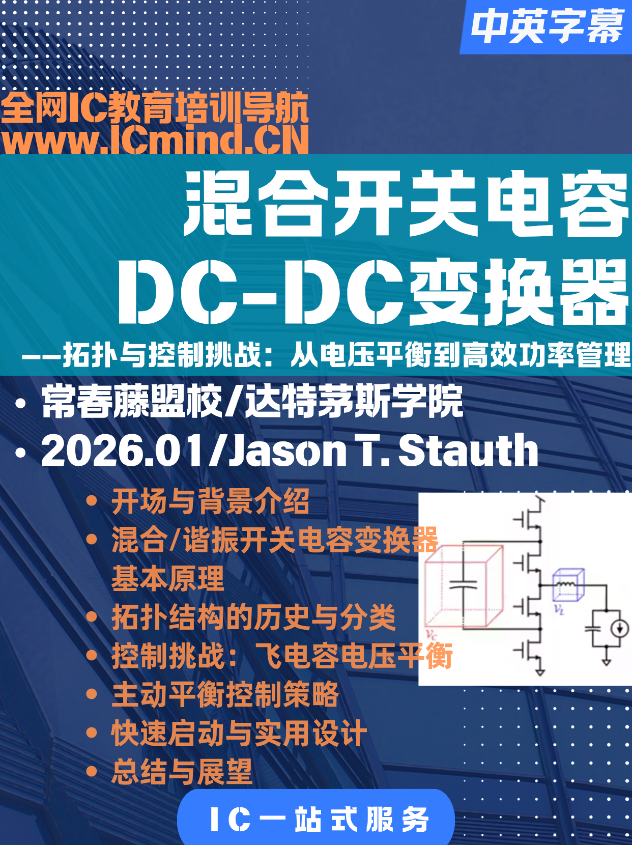
混合开关电容DC-DC变换器的拓扑与控制挑战——从电压平衡到高效功率管理
混合开关电容DC-DC变换器的拓扑与控制挑战——从电压平衡到高效功率管理
本讲座由达特茅斯学院JasonStealth教授主讲,深入探讨了混合/谐振开关电容DC-DC变换器的核心原理、拓扑分类与控制挑战。重点分析了飞电容电压平衡这一关键问题,介绍了基于现代控制理论的可观测性与可控性分析框架,以及多种主动平衡控制策略(如谷值电流控制、应力限制控制、改进纹波注入等),并展示了快速启动等实际应用案例。 大纲: 1.开场与背景介绍 2.混合/谐振开关电容变换器基本原理 3.拓扑结构的历史与分类 4.控制挑战:飞电容电压平衡 5.主动平衡控制策略 6.快速启动与实用设计 7.总结与展望 8.Q&A环节
完整版私信客服 186-6709-0885
【讲座】信号完整性介绍
【讲座】信号完整性介绍
信号完整性介绍;SI介绍
完整版私信客服 186-6709-0885
GaN氮化镓:驱动未来的半导体材料——从蓝光LED到功率电子的革命
GaN氮化镓:驱动未来的半导体材料——从蓝光LED到功率电子的革命
本视频全面介绍了21世纪最重要的半导体材料之一——氮化镓(GaN)。从基础原子结构出发,讲解氮化镓的宽禁带特性、高电子迁移率等核心优势,回顾了中村修二等科学家发明蓝光LED的历史突破,详细解析金属有机化学气相沉积(MOCVD)等制造工艺,并深入探讨高电子迁移率晶体管(HEMT)器件原理。视频还涵盖了氮化镓在光电子、功率电子、5G通信、雷达系统、航空航天及国防领域的广泛应用,最后展望了氮化镓技术的未来发展趋势与市场前景。
完整版私信客服 186-6709-0885
IEEE-研讨会-巴西-04-CMOS光接收机:从850nm到电信波长的全集成光通信前端——Filip Tavernier教授
IEEE-研讨会-巴西-04-CMOS光接收机:从850nm到电信波长的全集成光通信前端——Filip Tavernier教授
本视频为IEEE固态电路学会与电子器件学会巴西南部联合分会主办的杰出讲座系列之一,主讲人是来自比利时鲁汶天主教大学的Filip Tavernier教授。讲座系统阐述了基于标准CMOS工艺的光接收机设计前沿,内容涵盖光通信基础、850nm CMOS集成接收机、高速前端电路设计、1310/1550nm波段突破、实测结果与未来方向以及问答环节,适合光通信芯片设计工程师、模拟/射频IC设计师、光电集成领域研究人员及微电子专业研究生观看。
完整版私信客服 186-6709-0885
IEEE-研讨会-巴西-01-物联网低功耗电路:从能量收集到超宽带射频发射器
IEEE-研讨会-巴西-01-物联网低功耗电路:从能量收集到超宽带射频发射器
本视频是IEEE固态电路学会与电子器件学会巴西南部联合分会主办的杰出讲座系列之一,由葡萄牙里斯本大学高等技术学院的Jorge Fernández教授主讲。讲座系统阐述了面向物联网无线传感器节点的低功耗电路设计前沿,内容涵盖技术演进与驱动力、能量收集电路、超低功耗射频发射器以及问答环节,适合集成电路设计工程师、物联网研究人员、射频/模拟电路从业者及电子工程专业师生观看。
完整版私信客服 186-6709-0885
IEEE-研讨会-巴西-05-ADC性能极限:采样、量化与失配
IEEE-研讨会-巴西-05-ADC性能极限:采样、量化与失配
本视频为IEEE固态电路学会(SSCS)主办的杰出讲座系列之一。主讲人Marcel Pelgrom教授拥有41年产业经验,曾任飞利浦公司首席科学家,现任埃因霍温理工大学教授,是模拟/混合信号集成电路设计领域的国际权威。讲座深入剖析了模数转换器(ADC)面临的物理与电路基础极限,适合ADC设计工程师、模拟/混合信号IC设计师、射频前端工程师、集成电路专业研究生及高年级本科生观看。
完整版私信客服 186-6709-0885
IEEE-研讨会-《从语言到电路:Agentic AI、基础模型与开源EDA前沿研讨会》
IEEE-研讨会-《从语言到电路:Agentic AI、基础模型与开源EDA前沿研讨会》
本次由IEEE固态电路协会(SSCS)主办的研讨会,聚焦人工智能与集成电路设计的交叉前沿,来自多所高校及英伟达等机构的顶尖学者与产业专家,系统探讨了大型语言模型(LLM)在数字/模拟/射频电路设计中的最新突破。
完整版私信客服 186-6709-0885
【IEEE研讨会】PMIC设计与优化_2025.11.17
【IEEE研讨会】PMIC设计与优化_2025.11.17
PMIC设计流程与实用技术:从拓扑选择到自动化测试的完整指南 视频简介 本视频由加州大学圣地亚哥分校(UCSD)李教授主讲,面向初级工程师及其他领域有经验但对集成电源转换器设计感兴趣的工程师,系统介绍集成电源管理IC(PMIC)的完整设计流程。 演讲首先阐述了集成电源转换器的应用背景与动机,从智能手机主板中大量占据面积的被动元件出发,说明集成化、小型化的必要性。随后深入讲解核心设计环节:包括Buck/Boost等拓扑选择、开关管在深度线性区的特性分析、基于Plexim的仿真与损耗计算、开关尺寸优化方法;重点剖析了栅极驱动器设计(扇出系数选择)、ESD保护策略;并详细展示版图设计中的关键考量——从晶体管 finger 布局、通孔与金属层堆叠以降低寄生电阻,到电源网格规划与倒装芯片封装优势。最后介绍PCB设计与自动化测试平台的搭建,演示如何远程控制数千个测试点实现高效验证。 问答环节还涉及SIMO架构的交叉调整率、输入阻抗影响、功率管 finger 宽度优化、寄生电感抑制策略,以及面向NVIDIA GPU等高性能计算场景的大电流供电挑战。 关键词 集成电源转换器、PMIC设计、电源管理IC、DC-DC变换器、Buck变换器、Boost变换器、开关电容变换器、混合变换器、栅极驱动器、版图设计、寄生电阻、通孔优化、电源网格、倒装芯片、自动化测试、SIMO转换器、交叉调整率、ESD保护、损耗分析、Plexim仿真、高性能计算供电、电流密度优化
完整版私信客服 186-6709-0885
[ADC]澳门大学-陈知行-SAR ADC 中冗余位的作用
[ADC]澳门大学-陈知行-SAR ADC 中冗余位的作用
本视频主要讲解常规 SAR ADC 中冗余位的用途。首先回顾了 ADC 的模型,包括 ADC 的定义、输入噪声与量化。为模拟冗余位的影响,对 SAR 功能进行了修改,引入冗余位以应对位周期加速时的不完全建立误差。因建立过程难以建模,故采用不完全建立导致错误比较结果这一后果,并引入新变量表示错误比较概率(1 为完全正确,0 为完全错误)。通过分析理想条件下的模型结果,阐述了添加冗余位前后残差误差的变化以及对信噪比的影响,最终说明添加冗余位可使残差误差重新被限制在特定范围内。
完整版私信客服 186-6709-0885
[ADC]SAR ADC中冗余位的作用-MATLAB 澳门大学-陈知行
[ADC]SAR ADC中冗余位的作用-MATLAB 澳门大学-陈知行
本视频主要介绍如何在MatLab模型中添加增益失配、偏移和时序偏差这三种非理想因素,并观察它们对输出频谱的影响。
完整版私信客服 186-6709-0885
[SerDes]ECEN720-2025-发射前馈均衡(TX FFE)对高速信道性能的影响分析
[SerDes]ECEN720-2025-发射前馈均衡(TX FFE)对高速信道性能的影响分析
标题:Homework 4解决方案:发射前馈均衡(TX FFE)对高速信道性能的影响分析 简介 本内容是关于Homework 4的解决方案讲解,主要研究在1米直连铜缆、特定PCB走线和封装的信道中,不同发射前馈均衡(TX FFE)配置对信号性能的影响。具体包括在28 Gbit/s(14 Gsymbol/s)和80 Gbit/s(40 Gsymbol/s)两种数据速率下,采用无均衡、2抽头(1主1后)、5抽头(1前1主3后)和10抽头(2前1主7后)四种FFE配置,并对比理想未量化抽头权重与6比特量化抽头权重的性能差异,通过脉冲响应峰值失真眼高和随机数据眼高来评估。 大纲 1. 作业概述:介绍Homework 4的研究对象(特定信道)、目标(研究TX FFE影响)及关键参数(四种FFE配置、两种数据速率、量化与未量化抽头)。 2. FFE抽头选择方法:提及采用最小均方误差(MMSE)方法(参考 Lecture 4 Slide 12)。 3. 28 Gbit/s PAM4性能分析: 不同FFE配置的峰值失真眼高对比(未量化与量化)。 2抽头FFE:通过Matlab代码演示,未量化与量化抽头眼高相近,脉冲响应有效抑制后光标ISI,眼图张开。 10抽头FFE:未量化抽头部分值小,6比特量化后部分抽头归零,性能接近6抽头;未量化眼图更干净,量化眼图也能张开;脉冲响应后光标ISI基本被消除;性能在约6抽头时饱和。 4. 80 Gbit/s PAM4性能分析: 2抽头FFE:眼图仍闭合,脉冲响应虽抑制后光标ISI,但前光标ISI是主要问题。 10抽头FFE:未量化抽头眼高约10mV,量化后眼高约25mV且眼图更干净;脉冲响应能处理前、后光标ISI,但信号幅度被大幅降低;量化抽头性能可能接近7抽头。 5. 其他观察:量化可能导致抽头值非单调变化。 关键词 Homework 4, TX FFE (发射前馈均衡), 信道, 铜缆, PCB走线, PAM4, 数据速率, 28 Gbit/s, 80 Gbit/s, 抽头配置, 未量化抽头, 6比特量化, 眼图, 眼高, 脉冲响应, ISI (码间干扰), MMSE (最小均方误差)
完整版私信客服 186-6709-0885
[SerDes]ECEN720-2025-高速有线收发器设计及未来挑战探讨
[SerDes]ECEN720-2025-高速有线收发器设计及未来挑战探讨
标题:高速有线收发器设计及未来挑战探讨 简介 Sam教授(德克萨斯农工大学)分享了其在模拟混合信号IC设计,尤其是有线收发器领域的研究经历,介绍了即将开展的相关培训课程内容,该课程与ISCC、CICC等顶级会议上的最新研究成果紧密结合,涵盖高速收发器架构、关键模块晶体管级实现、未来发展挑战及目标受众等方面。 大纲 1. 个人背景与研究兴趣:Sam教授自2009年起任德克萨斯农工大学教授,领导模拟混合信号IC设计研究组,专长有线收发器;曾就职于英特尔先进设计组,从事电气和光学有线收发器研究;于斯坦福大学获得博士学位,研究方向为片上芯片通信的光学收发器。 2. 课程与顶级会议的关联:课程与ISCC、CICC等精英会议的最新研究成果高度契合,例如ISCC上展示的200Gbps以上长距离收发器,以及CICC上Broadcom将展示的先进收发器,课程将涵盖这些收发器中的DSP、高速DAC发射器、大规模时间交织ADC前端等概念。 3. 课程主要亮点:包括高速(200Gbps以上)收发器架构分析(应对高频下的高信道损耗、严格时钟抖动规格等)、主要模块的晶体管级实现(高速DAC发射器、高性能模拟接收器前端、高速时间交织ADC、数字均衡实现、高性能时钟电路),以及光学收发器前端(用于远距离通信)。 4. 有线通信的未来挑战与发展方向:200Gbps以上,特别是448Gbps以太网速率面临信道带宽不足、有效奈奎斯特频率处损耗大等问题;需考虑替代调制方案(如高级多音或多载波信号、高阶PAM);电路方面需实现极高带宽前端(发射机和接收机前端的高级带宽扩展技术)、高效时间交织ADC架构;最终解决方案可能是共封装光学收发器(如Broadcom的大型交换芯片)。 5. 课程目标受众:主要为有一定300mm工艺经验,希望学习当前高性能系列收发器架构先进设计技术的模拟混合信号IC设计工程师;对该领域感兴趣的任何人,课程将从基础开始,逐步过渡到高级技术,并参考关键文献。 关键词 有线收发器,模拟混合信号IC设计,高速DAC发射器,时间交织ADC,数字均衡,时钟电路,调制方案,共封装光学收发器,ISCC,CICC,200Gbps,448Gbps
完整版私信客服 186-6709-0885
[SerDes]ECEN720-2025-高性能serdes设计:200Gbps传输技术概述
[SerDes]ECEN720-2025-高性能serdes设计:200Gbps传输技术概述
标题:高性能serdes设计:200Gbps传输技术概述 简介 本文是关于高性能serdes设计中200Gbps传输技术的概述,主要介绍了模拟串行收发器链路的基本框图、面临的挑战及解决方案。内容涵盖了关键的通道特性、通信技术、均衡实现(包括发射端前馈均衡和接收端连续时间线性均衡、判决反馈均衡等)、基于ADC的接收器、时钟生成与分配以及光收发器等方面,还提及了课程将在后续各讲座中深入探讨的相关主题。 大纲 1. 模拟串行收发器链路基本介绍 - 功能:发射端并行转串行、经通道传输、接收端串行转并行 - 挑战:通道的频率相关损耗特性(低通特性) 2. 均衡技术 - 发射端:前馈均衡(FIR),面临输出摆幅限制需衰减低频内容(去加重),随着抽头数增加,采用DSP计算FIR后接基于DB的输出级是更好方案(例:224Gbps发射器) - 接收端:连续时间线性均衡(例:224Gbps Pam4基于反相器的前端) 3. 基于ADC的接收器 - 原因:Pam4调制对残余ISI更敏感,需精确均衡,模拟域难实现,ADC量化前端输出以便数字域进行ISI消除 - 问题:ADC和数字均衡器功耗是主要问题 - 高速ADC设计:多秩采样、时间交织架构(例:8路时间交织设计,异步SAR架构单元ADC) 4. 时钟生成与分配 - 重要性:高频、低抖动 - 例:数字分数N基时钟生成(28GHz四分之一速率时钟),采用电流复用耦合倍频振荡器和分流串联时钟分配缓冲器 - 时钟数据恢复:基于ADC的PLL CDR,数字环路滤波器,B速率mu-mu鉴相器,控制八分之一速率PCO等 5. 光收发器 - 应用:数据中心扩展覆盖范围 - 热门技术:共封装光子收发器(基于微环调制器和滴滤器),支持波分复用,功率效率高(例:32通道WDM实现,英伟达200Gbps Pam4收发器) 6. 课程后续讲座安排:将分别深入探讨关键通道特性和通信技术(讲座1)、关键CES发射器和均衡主题(讲座2、4)、接收器和模拟均衡主题(讲座3、5)、时间交织ADC设计问题和数字均衡(讲座6)、时钟电路(讲座7)、光发射器前端(讲座8) 关键词 高性能serdes设计、200Gbps、模拟串行收发器链路、频率相关损耗、均衡技术、前馈均衡(FIR)、连续时间线性均衡、判决反馈均衡、Pam4调制、基于ADC的接收器、高速ADC、时间交织、时钟生成与分配、低抖动、时钟数据恢复(CDR)、光收发器、共封装光子收发器、微环调制器、波分复用(WDM)
完整版私信客服 186-6709-0885
[SerDes]ECEN720-2025-基于DAC的发射机架构与高速PAM调制实现(电流/电压模式详解)
[SerDes]ECEN720-2025-基于DAC的发射机架构与高速PAM调制实现(电流/电压模式详解)
视频标题: 高性能SERDES设计:基于DAC的发射机架构与高速PAM调制实现(电流/电压模式详解) 视频简介: 本视频为Sam Palermo教授2025年《高性能SERDES设计》在线课程精讲,深入解析高速串行通信中基于DAC的发射机(TX)实现方案。课程系统讲解了电流模式与电压模式DAC发射机的架构设计、二进制加权与温度计编码的线性度优化、分段式(Segmented)DAC的工程权衡,以及码相关输出阻抗对信号完整性的影响。同时结合56G/112G/224G等前沿速率实例,剖析PAM-4/6/8及OFDM调制在实际芯片设计中的实现细节、FFE均衡配合与高低摆幅驱动器的选型考量。适合高速接口、模拟/混合信号IC设计及信号完整性工程师学习参考。 关键词: SERDES, DAC发射机, 高速串行通信, 电流模式DAC, 电压模式DAC, 分段式DAC, 温度计编码, 二进制加权, PAM-4, PAM-6, PAM-8, OFDM调制, 224G, 112G, 56G, FFE均衡, 信号完整性, 芯片设计, Sam Palermo, 发射机线性度, 输出阻抗匹配
完整版私信客服 186-6709-0885
[ADC]澳门大学-陈知行-时间交织ADC架构:原理、特性与挑战初探
[ADC]澳门大学-陈知行-时间交织ADC架构:原理、特性与挑战初探
本预览主要介绍了时间交织ADC(模数转换器)的基本架构、工作方式(包括非重叠和重叠跟踪时间)、显著优势(高速、功率可扩展、适合先进工艺)以及面临的主要局限性(通道失配、输入负载问题、重叠跟踪时间带来的线性度影响等),并通过四通道实例进行了说明,最后提及后续将深入探讨其非理想性及架构考量。
完整版私信客服 186-6709-0885
[ADC]澳门大学-陈知行-参考缓冲器架构设计与纹波抑制技术
[ADC]澳门大学-陈知行-参考缓冲器架构设计与纹波抑制技术
本课程为澳门大学C-H Chan教授讲授的"极限SAR ADC:探索新前沿"系列内容,深入探讨高速高精度SAR ADC设计中参考缓冲器的核心挑战与解决方案。课程分析了参考缓冲器的功耗瓶颈及三种关键缓冲器架构的权衡,剖析了参考电压纹波的产生机理及其影响,还系统梳理了五大类解决方案,为高性能ADC的参考电压设计提供完整思路与理论模型。
完整版私信客服 186-6709-0885
[2025-ESSERC]PMIC-英飞凌-功率与性能效率:从数据中心到自动驾驶汽车再到人形机器人的电源管理创新
[2025-ESSERC]PMIC-英飞凌-功率与性能效率:从数据中心到自动驾驶汽车再到人形机器人的电源管理创新
英飞凌系统架构师Frank Praemassing在演讲中深入探讨了功率管理技术在现代电子系统中的核心作用及创新挑战,涵盖数据中心AI算力爆炸的能效挑战、软件定义汽车架构转型的智能电源管理,以及人形机器人这一新兴物理AI应用的技术需求,并分析了相关技术趋势,分享了职业经验,鼓励年轻工程师把握机遇。
完整版私信客服 186-6709-0885
[2025-ESSERC]PMIC-Bernhard Wicht-电源管理集成电路设计:从基础拓扑到AI时代的高性能应用
[2025-ESSERC]PMIC-Bernhard Wicht-电源管理集成电路设计:从基础拓扑到AI时代的高性能应用
视频标题: 电源管理集成电路设计:从基础拓扑到AI时代的高性能应用 视频简介: 本演讲由Bernhard Wicht博士主讲,系统介绍了电源管理IC设计的核心概念与发展趋势。内容涵盖:电源管理IC在现代电子系统中的关键作用、从线性稳压器到开关电源的四种主要电压转换拓扑、高功率AI处理器(如NVIDIA H100 GPU)的供电挑战、以及面向数据中心的48V供电架构。演讲还深入探讨了栅极驱动器、控制环路等关键电路设计,并展示了全集成混合转换器等前沿研究成果。适合对电源管理、功率电子和AI硬件基础设施感兴趣的工程师与研究人员观看。 关键词: 电源管理IC、DC-DC转换器、线性稳压器、开关电源、混合转换器、AI处理器供电、GPU电源设计、48V架构、栅极驱动器、多相Buck转换器、能量效率、无源元件集成、数据中心供电、开关电容转换器
完整版私信客服 186-6709-0885
![[DCDC]耦合电感如何提升大电流供电性能:建模、直觉与优化全解析](https://material-image.wanwang.xin/1597234105050516/public/d62d9057-e830-4720-86af-d52148ea604a.png)
[DCDC]耦合电感如何提升大电流供电性能:建模、直觉与优化全解析
[DCDC]耦合电感如何提升大电流供电性能:建模、直觉与优化全解析
基本概念与优势 多相BUCK的工作原理与局限性 磁耦合如何实现纹波消除与瞬态响应改善 电路模型:T模型、变压器模型与电流平衡变压器 磁路模型与电感对偶模型 关键参数分析:Gamma与Beta 优化设计方法:固定泄漏电感、最大化磁化电感 实现方案对比:侧向离散式、垂直供电式、TLVR、空气芯、片上薄膜磁芯 实际应用案例:Princeton垂直供电Lego系统、Intel全集成稳压器、Apple商用产品
完整版私信客服 186-6709-0885
![[LDO]清华大学-路延教授-LDO设计原理与关键技术预览](https://material-image.wanwang.xin/1597234105050516/public/50042ea2-b377-4800-979f-acc8c4c1cd07.png)
[LDO]清华大学-路延教授-LDO设计原理与关键技术预览
[LDO]清华大学-路延教授-LDO设计原理与关键技术预览
本讲由来自Tsinghua University的Yan Lu主讲,主要介绍了低压差线性稳压器(LDO)的基本概念、拓扑结构、设计中的关键问题(如反馈环路主极点的设置、稳定性考量),并探讨了多种缓冲器拓扑(如源极跟随器、超级源极跟随器、翻转电压跟随器FF)及其在LDO中的应用,最后提及将采用P控制系列理论及小信号、大信号分析方法来深入研究LDO设计。
完整版私信客服 186-6709-0885
![[LDO]清华大学-路延教授-LDO设计与分析培训课程介绍](https://material-image.wanwang.xin/1597234105050516/public/22e1f77e-4821-4314-8693-a7b88cb8263f.png)
[LDO]清华大学-路延教授-LDO设计与分析培训课程介绍
[LDO]清华大学-路延教授-LDO设计与分析培训课程介绍
采访内容涉及教授的背景、课程动机、课程内容、课程亮点、特定设计项目以及课程目标受众等。通过这次采访,读者可以了解到即将开设的课程将如何帮助工程师们提升在高性能LDO电路设计方面的知识和技能。
完整版私信客服 186-6709-0885
![[LDO]清华大学-路延教授-LDO的PSR分析:基于米勒补偿与功率晶体管栅极主导极点](https://material-image.wanwang.xin/1597234105050516/public/e9a73333-f3dc-4d9e-8e98-efa8d1d23865.png)
[LDO]清华大学-路延教授-LDO的PSR分析:基于米勒补偿与功率晶体管栅极主导极点
[LDO]清华大学-路延教授-LDO的PSR分析:基于米勒补偿与功率晶体管栅极主导极点
主要讨论了带有Miller补偿的LDO的电源抑制比(PSR)分析,特别是当主导极点位于功率晶体管的栅极或EA输出时的情况。
完整版私信客服 186-6709-0885
![[LDO]清华大学-路延教授-如何优化LDO的瞬态响应](https://material-image.wanwang.xin/1597234105050516/public/bb20dc57-2f39-4893-a263-e9fa82710813.png)
[LDO]清华大学-路延教授-如何优化LDO的瞬态响应
[LDO]清华大学-路延教授-如何优化LDO的瞬态响应
本内容聚焦于电容式LDO(低压差线性稳压器)的设计。传统PMIC中集成DCDC转换器和LDO存在引脚消耗多以及LDO远离负载时性能(瞬态响应、电源抑制等)不佳的问题,因此催生了对电容式LDO的需求。然而,设计高性能(良好瞬态响应和电源抑制)的电容式LDO面临诸多挑战。内容还介绍了“Capacitor-Free SIMO Audio with Damping Factor Control Technique”等经典论文中的技术,包括阻尼因子控制补偿技术、多级LDO设计、跨导(GM)提升级、以及反馈电阻网络中的电容CF等,探讨了这些技术如何应对稳定性、带宽、相位裕度等问题,并提及了开环LDO及其在数字电路系统中的应用和优缺点,如稳定性、输出电压随负载电流变化以及DC负载线技术带来的瞬态性能改善等。 ## 大纲
完整版私信客服 186-6709-0885
224G SerDes与1.6TE测试新趋势解析-2025.08-VIAVI Solutions ×翔宇科技
224G SerDes与1.6TE测试新趋势解析-2025.08-VIAVI Solutions ×翔宇科技
本视频深入探讨数据中心高速互联技术的最新发展趋势,重点分析从50G、112G、224G向448G演进的驱动力与技术挑战。演讲者详细阐述了"海滩前沿带宽"概念,解析AI时代下芯片面积与I/O带宽的错配问题,以及Tomahawk 6等新一代交换芯片带来的100Tbps级带宽需求。视频涵盖1.6T光模块的市场爆发、OSFP封装技术、链路训练(LT)等新特性,并分享了224G PAM4信号完整性测试的第一手经验与关键洞察,最后展望448G及CPO/共封装光学等前沿技术方向。
完整版私信客服 186-6709-0885
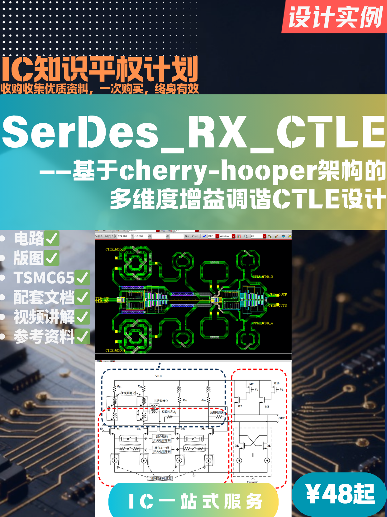
基于cherry-hooper架构的多维度增益调谐CTLE设计
基于cherry-hooper架构的多维度增益调谐CTLE设计
基于cherry-hooper架构的多维度增益调谐CTLE设计 202X年集创赛国家二等奖作品 1、架构创新,采用cherry-hooper架构 2、绘制电感,非PDK电感,工艺:T65nm 3、PDF文档50页-原理分析+电路设计+仿真解析,+PPT11页汇报,+讲解视频20分钟 关键词:serdes;接收机;RX;CTLE;高速串行接口接收机模拟前端;T线圈峰化技术;阻抗分析;三谐振峰化;负电容补偿技术;二端口网络分析;增益调节;开关电阻阵列;开关电容阵列;
完整版私信客服 186-6709-0885
ADS Python教程-1 Python控制台入门
ADS Python教程-1 Python控制台入门
本视频是ADS Python教程系列第一集,旨在带用户快速上手Keysight ADS中的Python控制台功能。核心内容包括ADS Python API文档快速导览、使用Python脚本创建工作空间、创建并添加自定义库到工作空间以及从GUI操作到Python自动化的思维转换。适合希望用Python自动化ADS设计流程的射频/微波工程师、想提升效率的ADS用户及对ADS脚本开发感兴趣的初学者,前置要求为ADS 2025或更高版本及基础Python编程知识。视频将详细讲解ADS设计环境Python API使用方法,示例代码可在视频描述博客链接获取,后续教程将涉及原理图创建等进阶内容。
完整版私信客服 186-6709-0885
![[SI]从眼图一眼看穿信号完整性问题:反射、串扰、损耗的诊断与仿真实战](https://material-image.wanwang.xin/1597234105050516/public/ba60bd1c-d6e4-42fa-8546-f1dfb2bd1e60.png)
[SI]从眼图一眼看穿信号完整性问题:反射、串扰、损耗的诊断与仿真实战
[SI]从眼图一眼看穿信号完整性问题:反射、串扰、损耗的诊断与仿真实战
大纲 眼图是如何生成的? 眼图的“健康标准”:张开与闭合 问题诊断 Part 1:反射 (Reflection) Part 2:串扰 (Crosstalk) Part 3:损耗 (Loss) 进阶话题:均衡 (Equalization)
完整版私信客服 186-6709-0885
![[2025-CICC]高速有线接收机电路基础:从ESD保护到T型线圈的带宽扩展技术](https://material-image.wanwang.xin/1597234105050516/public/c65ea357-aad1-4e46-ad40-21fa62b077a8.png)
[2025-CICC]高速有线接收机电路基础:从ESD保护到T型线圈的带宽扩展技术
[2025-CICC]高速有线接收机电路基础:从ESD保护到T型线圈的带宽扩展技术
本视频由MediaTek的Miguel Gandara博士主讲,系统介绍高速有线通信接收机的前端电路设计。内容涵盖两大核心模块:输入网络(ESD保护结构与宽带阻抗匹配)和连续时间线性均衡器(CTLE)。重点讲解如何通过T型线圈(T-coil)等无源网络突破RC带宽限制,实现从8GHz到"无限带宽"的扩展,以及串联电感补偿技术的权衡考量。演讲特别强调时域仿真的重要性——AC带宽并非一切,群延迟波动和阶跃响应才是评估电路性能的关键指标。适合对高速SerDes、模拟/混合信号设计感兴趣的工程师和学生。
完整版私信客服 186-6709-0885
![[2025-CICC]高速有线发射机电路基础:从数据洪流到224G SerDes设计](https://material-image.wanwang.xin/1597234105050516/public/5083692a-7f12-47e0-bbbe-af1a01cca771.png)
[2025-CICC]高速有线发射机电路基础:从数据洪流到224G SerDes设计
[2025-CICC]高速有线发射机电路基础:从数据洪流到224G SerDes设计
本视频由Synopsys高级经理Noman Hay博士主讲,系统介绍高速有线通信中SerDes发射机电路的核心原理与设计要点,涵盖数据中心通信需求、串并通信对比、SerDes系统架构、信道特性与眼图分析、调制技术、驱动电路、前馈均衡技术及数字辅助发射机发展趋势,适合集成电路设计、高速通信领域的工程师与研究人员学习参考。
完整版私信客服 186-6709-0885
![[2025-CICC]从简单到超级源极跟随器:模拟电路设计的核心直觉](https://material-image.wanwang.xin/1597234105050516/public/f939983c-80d0-4118-8e36-2073d358fd66.png)
[2025-CICC]从简单到超级源极跟随器:模拟电路设计的核心直觉
[2025-CICC]从简单到超级源极跟随器:模拟电路设计的核心直觉
本讲座由多伦多大学教授、IEEE SSCS"电路直觉"专栏作者主讲,系统讲解模拟IC设计中源极跟随器的演进历程。从基础概念出发,逐步深入分析四种关键电路拓扑:简单源极跟随器、翻转电压跟随器(FVF)、超级源极跟随器(SSF)以及Class AB超级源极跟随器。特别适用于本科高年级学生及研究生,帮助建立从第一性原理分析模拟电路的直觉思维。
完整版私信客服 186-6709-0885
![[2025-CICC]高速有线接收机电路基础:从ESD保护到T型线圈的带宽扩展技术](https://material-image.wanwang.xin/1597234105050516/public/408c0594-514d-490e-8904-029adeba3a83.png)
[2025-CICC]高速有线接收机电路基础:从ESD保护到T型线圈的带宽扩展技术
[2025-CICC]高速有线接收机电路基础:从ESD保护到T型线圈的带宽扩展技术
本视频由MediaTek的Miguel Gandara博士主讲,系统介绍高速有线通信接收机的前端电路设计。内容涵盖两大核心模块:输入网络(ESD保护结构与宽带阻抗匹配)和连续时间线性均衡器(CTLE)。重点讲解如何通过T型线圈(T-coil)等无源网络突破RC带宽限制,实现从8GHz到"无限带宽"的扩展,以及串联电感补偿技术的权衡考量。演讲特别强调时域仿真的重要性——AC带宽并非一切,群延迟波动和阶跃响应才是评估电路性能的关键指标。适合对高速SerDes、模拟/混合信号设计感兴趣的工程师和学生。
完整版私信客服 186-6709-0885
![IEEE-研讨会-印度-06-[ADC]-MATLAB混合信号IC优化设计:从晶体管级设计优化到ADC系统级性能提升](https://material-image.wanwang.xin/1597234105050516/public/50eaa948-38a5-4191-a6bc-725838d0f862.png)
IEEE-研讨会-印度-06-[ADC]-MATLAB混合信号IC优化设计:从晶体管级设计优化到ADC系统级性能提升
IEEE-研讨会-印度-06-[ADC]-MATLAB混合信号IC优化设计:从晶体管级设计优化到ADC系统级性能提升
本视频由MathWorks工程师Janvi主讲,系统介绍如何利用MATLAB和Simulink工具进行混合信号集成电路(Mixed-Signal IC)的设计优化与性能提升。
完整版私信客服 186-6709-0885
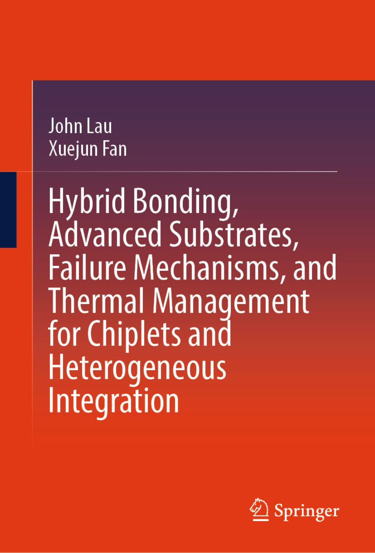
【教材】Hybrid Bonding, Advanced Substrates, Failure Mechanisms, and Thermal Management for Chiplets and Heterogeneous Integration
【教材】Hybrid Bonding, Advanced Substrates, Failure Mechanisms, and Thermal Management for Chiplets and Heterogeneous Integration
本书聚焦于小芯片和异构集成的设计、材料、工艺、制造、失效机制、可靠性、建模和热管理。既探讨了原理,也涉及了工程实践,但更侧重于工程实践。通过深入研究混合键合、先进基板、失效机制、热应力导致的建模、吸湿、跌落等冲击载荷以及电流驱动的电迁移等若干重大主题,以及热管理的基本原理,实现了这一目标。每个主题都进行了深入分析,以将基础原理与现实世界的工程挑战联系起来。本书是电气工程、机械工程、材料科学和工业工程领域的研究人员、工程师和学生的必备资源,为他们提供了推动半导体封装和集成创新所需的知识。
完整版私信客服 186-6709-0885
![IEEE-研讨会-印度-05-[LDO]系统化设计LDO的挑战:gm/ID方法论在模拟IC设计中的应用与局限](https://material-image.wanwang.xin/1597234105050516/public/293b2bf9-8605-4e59-9483-41d73bac15b6.png)
IEEE-研讨会-印度-05-[LDO]系统化设计LDO的挑战:gm/ID方法论在模拟IC设计中的应用与局限
IEEE-研讨会-印度-05-[LDO]系统化设计LDO的挑战:gm/ID方法论在模拟IC设计中的应用与局限
本视频由斯坦福大学博士、曾任职于德州仪器和苹果的Sakshi Aurora博士主讲,深入探讨模拟IC设计中系统化方法的重要性与挑战。以LDO为案例,系统介绍了系统化设计的原因、gm/ID方法论、LDO系统化设计流程及面临的实际挑战,适合模拟IC设计初学者、在校学生及资深工程师,还涉及机器学习在模拟电路设计中的应用前景和开源模拟IC设计的重要性。
完整版私信客服 186-6709-0885
【课程】CDR 台大 李致毅老师
【课程】CDR 台大 李致毅老师
视频简介 本系列课程系统讲解时钟数据恢复电路(CDR)的核心原理与进阶设计,是高速有线通信与SERDES系统设计的深度技术指南。 课程从CDR与锁相环(PLL)的紧密关联出发,阐述CDR在有线通信(光纤、电缆、背板)中的核心任务——从失真数据流中恢复干净数据并重建同步时钟。内容深入剖析基于PLL的主流CDR架构,详细对比线性(Hogge)、纯线性(Purely Linear)与Bang-Bang(ALEXANDER/BENBEN)三大鉴相器的工作原理、特性差异、速度极限与适用场景;并进一步探讨双环频率捕获架构、亚速率(Half-Rate/Quarter-Rate)设计、DLL/相位内插器(PI)架构、全数字CDR及过采样技术。 针对PON/FTTH等突发通信场景,课程还涵盖Burst Mode快速锁定方案(Gated VCO、Injection Locked CDR)。最后系统分析CDR的关键抖动指标——抖动传输(Jitter Transfer)、抖动容限(Jitter Tolerance)与抖动生成(Jitter Generation),揭示线性CDR与Bang-Bang CDR在抖动性能上的本质差异,为高速串行通信接收端设计提供完整的理论支撑与工程实践指导。 关键词 时钟数据恢复(CDR)、锁相环(PLL)、SERDES、有线通信、鉴相器(PD)、Hogge PD、Bang-Bang PD、ALEXANDER鉴相器、纯线性鉴相器、电荷泵、环路滤波器、VCO、频率检测器(FD)、双环架构、亚速率(Sub-Rate)、半速率(Half-Rate)、四分之一速率(Quarter-Rate)、相位内插器(PI)、延迟锁定环(DLL)、全数字CDR、过采样(Over-Sampling)、Burst Mode、突发模式、Gated VCO、注入锁定(Injection Locking)、抖动传输(Jitter Transfer)、抖动容限(Jitter Tolerance)、抖动生成(Jitter Generation)、NRZ数据流、时钟重建、数据重定时、均衡器(DFE/FFE)、高速串行通信、频率捕获、锁定范围、尼奎斯特采样
完整版私信客服 186-6709-0885
【教材】GaN Power Devices for Efficient Power Conversion_2025
【教材】GaN Power Devices for Efficient Power Conversion_2025
氮化镓晶体管设计与应用的最新简明综述 在新修订的《高效功率转换用氮化镓功率器件》第四版中,由杰出研究人员和资深工程师组成的团队提供了一份简洁有效的新指南,指导如何使用氮化镓晶体管设计小型、节能且经济的产品。此新版涵盖了所有相关的氮化镓技术新进展,使学生和执业工程师能够掌握并领先于氮化镓器件及电路技术的发展。 您将探索包括直流-直流转换器、太阳能逆变器、电机驱动控制器、卫星电子设备和激光雷达设备在内的应用。第四版针对空间应用、垂直氮化镓以及驱动晶体管和集成电路进行了重要更新。关于可靠性测试进展、器件老化机制、热管理以及单片集成最新发展的新章节完善了本书内容。 读者还将发现: 关于集成电路、可靠性研究和新应用等重大技术改进的最新更新 对集成电路构造、特性、可靠性结果和应用的全面探讨 关于设计功率转换系统时特定电路设计、布局和热耗散的实用讨论 由功率半导体领域的资深专家领袖和行业先驱撰写的章节 《高效功率转换用氮化镓功率器件》非常适合从事功率转换工作的工程师,也将使电力电子领域的电气工程学生和器件科学家受益。
完整版私信客服 186-6709-0885
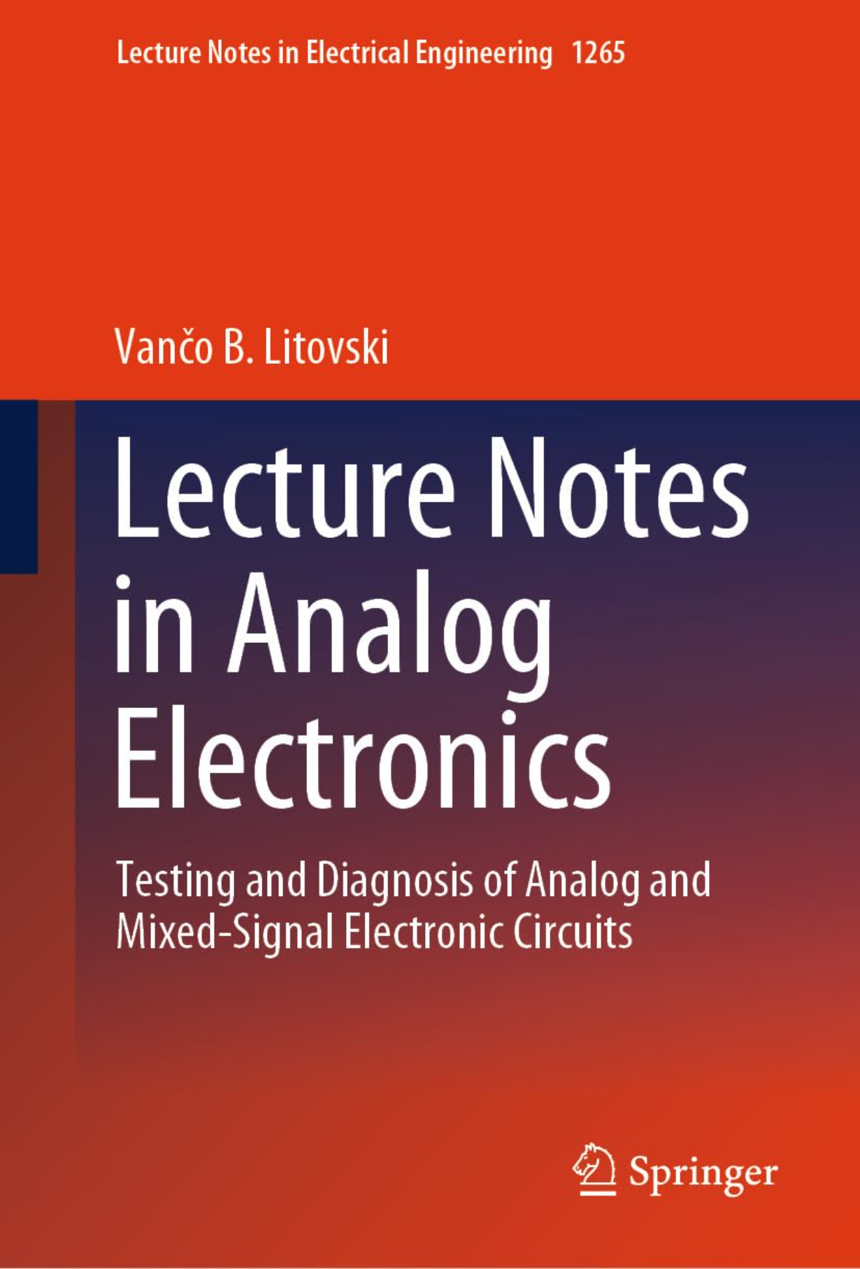
【教材】Lecture Notes in Analog Electronics
【教材】Lecture Notes in Analog Electronics
本书主要致力于模拟信号的放大。它涵盖了不同的技术(双极型、MOS和MES)以及不同的频率范围,但始终处理小信号。电子系统中处理的模拟信号可能有多种来源。其中包括来自传感器的信号(机电、电磁、电化学、电声、电光等)、来自天线的由另一电子系统产生或 simply 宇宙产生的信号,以及电子系统内部产生的信号。大多数信号的共同特性是幅度小。在许多情况下,其幅度低于微伏。由于在系统输出端我们最常需要高幅度信号,因此电子系统在进行任何进一步处理之前采取的主要操作就是放大。
完整版私信客服 186-6709-0885
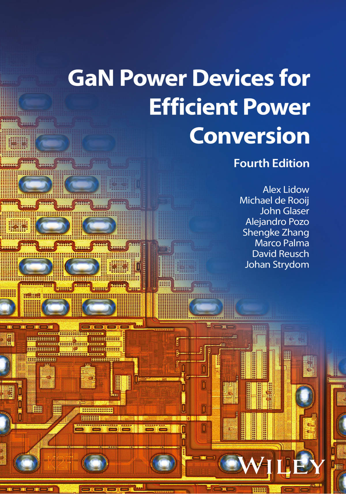
【教材】GaN Power Devices for Efficient Power Conversion_2025
【教材】GaN Power Devices for Efficient Power Conversion_2025
氮化镓晶体管设计与应用的最新简明综述 在新修订的《用于高效功率转换的氮化镓功率器件》第四版中,一组杰出的研究人员和实践工程师提供了一份简洁有效的新指南,指导如何使用氮化镓晶体管设计小型、节能且廉价的产品。此新版涵盖了所有相关的氮化镓技术新进展,使学生和实践工程师能够了解并领先于氮化镓器件和电路技术的发展。 您将探索包括直流-直流转换器、太阳能逆变器、电机驱动控制器、卫星电子设备和激光雷达设备在内的应用。第四版针对空间应用、垂直氮化镓以及驱动晶体管和集成电路进行了重要更新。关于可靠性测试进展、器件磨损机制、热管理以及单片集成最新发展的新章节完善了本书内容。 读者还将发现: 关于集成电路、可靠性研究和新应用等重大技术改进的最新更新 对集成电路构造、特性、可靠性结果和应用的全面探讨 关于设计功率转换系统时特定电路设计、布局和热耗散的实用讨论 由功率半导体领域的实践专家领导者和行业先驱撰写的章节 《用于高效功率转换的氮化镓功率器件》非常适合实践中的功率转换工程师,也将使电力电子领域的电气工程学生和器件科学家受益。
完整版私信客服 186-6709-0885
【教材】Analysis and Design of Data Converters
【教材】Analysis and Design of Data Converters
通过这本权威教科书掌握数据转换器设计的艺术,它是一份详细且易于理解的入门读物,非常适合学生和执业工程师。拉扎维独特且直观的教学方法,从基本组件逐步构建到复杂系统。逐步的晶体管级设计和仿真提供了对关键设计概念的实际动手理解。全面涵盖基本主题,包括采样电路、比较器设计、数模转换器、闪存拓扑结构、逐次逼近寄存器(SAR)和流水线架构、时间交错转换器以及过采样系统。超过250个示例提出发人深省的问题,强化核心概念并帮助学生建立信心。超过350道章末作业题用于测试学生的理解,课程教师可获得参考答案。由知名作者贝赫扎德·拉扎维编写,涵盖了当今工程师必不可少的所有原理和设计概念,这是理想的高年级本科生、研究生以及渴望在数据转换器分析和设计方面表现出色的专业工程师的教材。
完整版私信客服 186-6709-0885
【教材】Bulk-Driven Circuit Techniques for CMOS FDSOI Processes
【教材】Bulk-Driven Circuit Techniques for CMOS FDSOI Processes
在以数字为中心的系统和应用主导的当代技术格局中,模拟前端信号处理的重要性仍然不可或缺。关键的模拟、混合信号或毫米波组件(如低噪声放大器、均衡器和数据转换器)的精度和性能,基本上由跨导、直流增益、器件匹配、线性度和时序精度等技术参数决定。 通过内在设计改进来增强这些参数面临重大挑战,并且使用最先进的电路设计技术在某些限度之外变得不可行。由于CMOS晶体管的性能受到根本限制,通常采用前台或后台校准方案来减轻MOS器件的局限性。然而,这些限制可以通过采用绝缘体上硅(SOI)CMOS技术实现的有源和无源体驱动电路得到有效解决。全耗尽绝缘体上硅(FD-SOI)CMOS技术提供了比标准体CMOS技术更优越的晶体管特性,具有更高的电气性能、更好的功率效率和更强的可扩展性。 本书全面分析了FD-SOI CMOS技术,介绍了在模拟、数字、混合信号和毫米波电路与系统中采用体偏置技术的设计方法和电路实现方面的关键创新。它解决了关键的晶体管限制,包括有限的晶体管增益、失调、失配、噪声和线性度等。 作者提供了详细的技术见解、数学建模、设计方法和电路实现,涵盖了使用静态和动态晶体管体偏置技术的电路进展。重点在于克服最先进电路的局限性,如有限的直流增益、带宽、匹配/精度和功率效率。这些性能指标通过数学建模进行了严格研究,并通过仿真验证,以及使用动态和静态体偏置架构进行了实验演示。
完整版私信客服 186-6709-0885
【教材】Fully-Integrated Low-Dropout Regulators
【教材】Fully-Integrated Low-Dropout Regulators
全面讨论了全集成低压差稳压器(LDO)的关键规格,涵盖了经典的模拟架构以及最先进的数字和开关控制方法,提供了各种LDO架构的设计见解和比较,帮助读者找到合适的架构
完整版私信客服 186-6709-0885
【教材】Bulk-Driven Circuit Techniques for CMOS FDSOI Processes
【教材】Bulk-Driven Circuit Techniques for CMOS FDSOI Processes
在以数字为中心的系统和应用占主导地位的当代技术格局中,模拟前端信号处理的重要性仍然不可或缺。关键的模拟、混合信号或毫米波组件(如低噪声放大器、均衡器和数据转换器)的精度和性能,从根本上由跨导、直流增益、器件匹配、线性度和时序精度等技术参数决定。 通过内在设计改进来增强这些参数面临重大挑战,并且在使用最先进的电路设计技术时,超过一定限度后便不再可行。由于CMOS晶体管的性能存在根本性限制,通常采用前台或后台校准方案来缓解MOS器件的局限性。然而,这些限制可以通过采用绝缘体上硅(SOI)CMOS技术实现的有源和无源体驱动电路得到有效解决。全耗尽绝缘体上硅(FD-SOI)CMOS技术相较于标准体CMOS技术具有更优异的晶体管特性,可提供增强的电气性能、更高的功率效率和更好的可扩展性。 本书对FD-SOI CMOS技术进行了全面分析,介绍了在模拟、数字、混合信号及毫米波电路与系统中采用体偏置技术的设计方法和电路实现方面的关键创新。它解决了关键的晶体管局限性,包括有限的晶体管增益、失调、失配、噪声和线性度等。 作者提供了详细的技术见解、数学建模、设计方法和电路实现,涵盖了使用静态和动态晶体管体偏置技术的电路进展。重点在于克服最先进电路的局限性,如有限的直流增益、带宽、匹配/精度和功率效率。这些性能指标通过数学建模进行了严格研究,并通过仿真验证,以及使用动态和静态体偏置架构进行了实验演示。
完整版私信客服 186-6709-0885
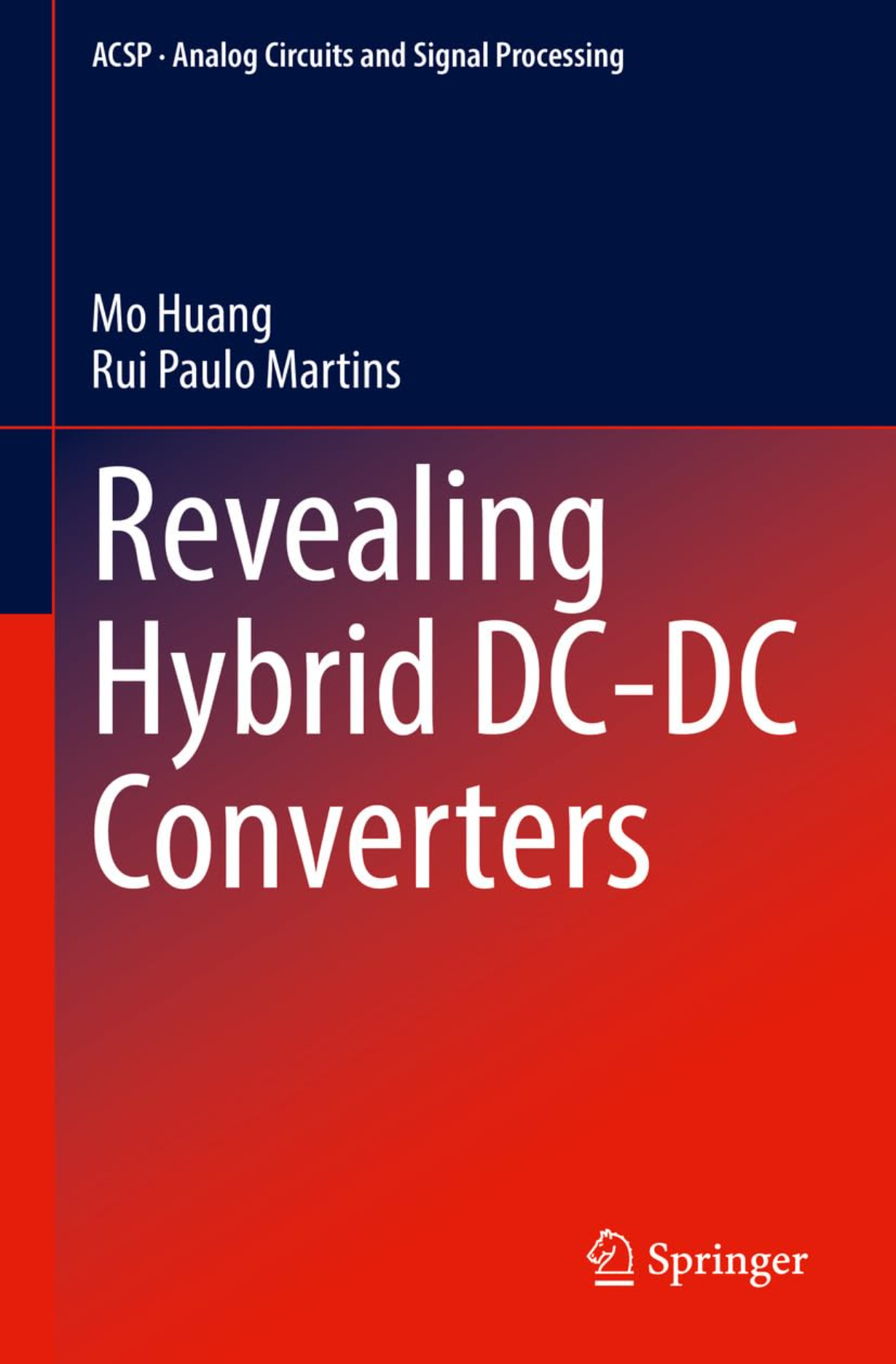
【教材】Revealing Hybrid DC-DC Converters (Analog Circuits and Signal Processing)
【教材】Revealing Hybrid DC-DC Converters (Analog Circuits and Signal Processing)
本书深入介绍了混合直流-直流转换器,这类转换器集成了电感器和电容器,以实现高效率和高功率密度。它们满足了高性能计算和汽车电子等应用的需求。尽管近年来的研究中已探索了多种混合转换器组合,但本书将指导读者为特定应用选择最佳拓扑结构。本书提供了对混合转换器的深刻理解,揭示了其潜在的设计理念。作者展示了多种流行混合转换器的示例,追溯了它们从简单的基本变压器模型发展而来的过程,同时强调了它们的优势和局限性。此外,本书还包含了发明新型混合转换器的设计指南。
完整版私信客服 186-6709-0885
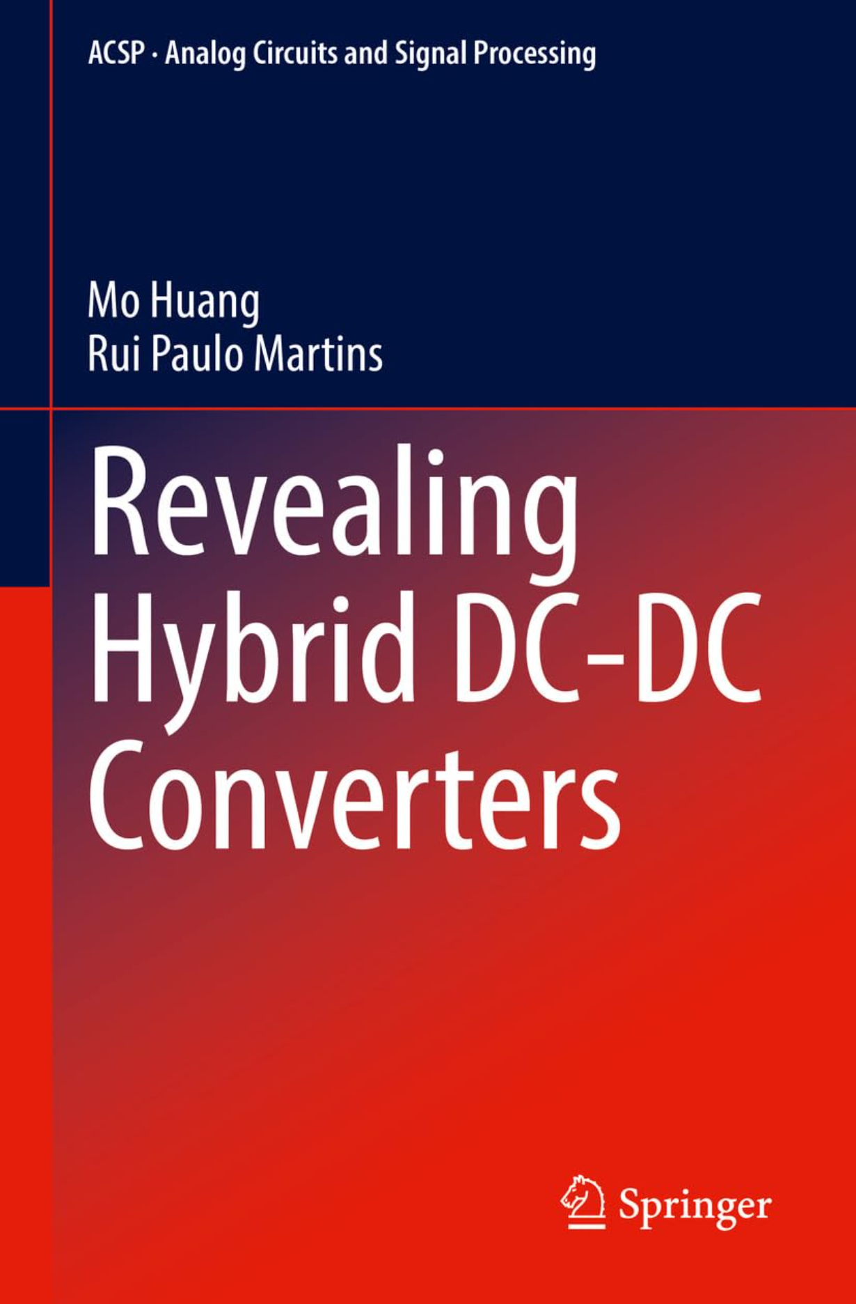
【教材】Revealing Hybrid DC-DC Converters (Analog Circuits and Signal Processing)
【教材】Revealing Hybrid DC-DC Converters (Analog Circuits and Signal Processing)
本书深入介绍了混合直流-直流转换器,这类转换器集成了电感器和电容器,以实现高效率和高功率密度。它们满足了高性能计算和汽车电子等应用的需求。尽管近年来的研究中已探索了多种混合转换器组合,但本书指导读者为特定应用选择最佳拓扑结构。本书对混合转换器提供了深刻的理解,揭示了其潜在的设计理念。作者展示了多个流行混合转换器的示例,追溯了它们从简单的基本变压器模型演变而来的过程,同时强调了它们的优势和局限性。此外,本书还包含了发明新型混合转换器的设计指南。
完整版私信客服 186-6709-0885
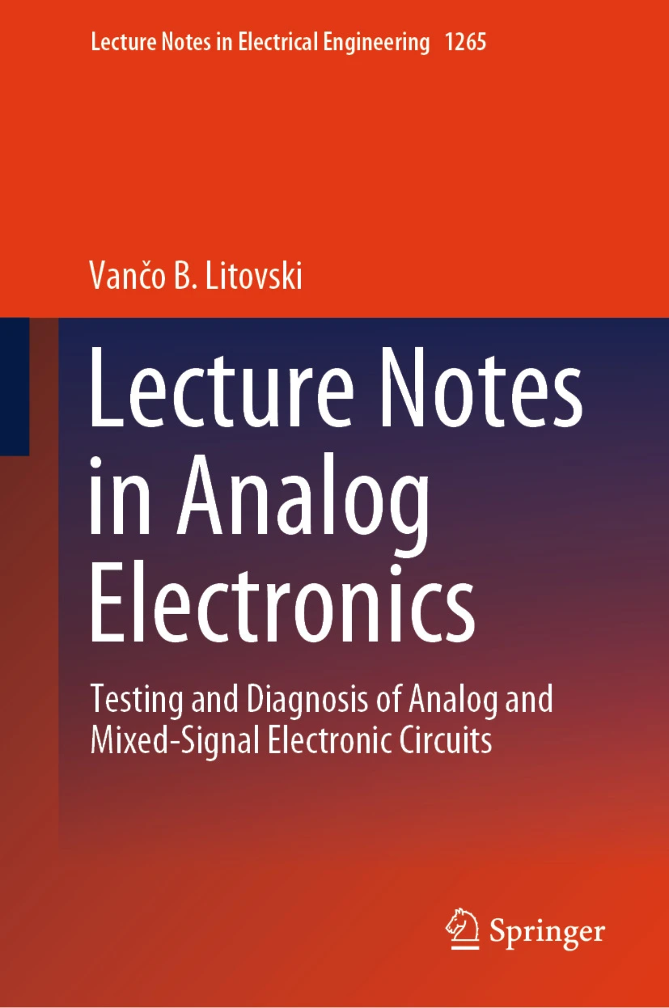
【教材】Lecture Notes in Analog Electronics
【教材】Lecture Notes in Analog Electronics
本书主要致力于模拟信号的放大。它涵盖了不同的技术(双极型、MOS和MES)以及不同的频率范围,但始终处理小信号。电子系统中处理的模拟信号可能有多种来源。其中包括来自传感器的信号(机电、电磁、电化学、电声、电光等),来自天线的信号(由另一个电子系统产生或 simply 由宇宙产生),以及在电子系统内部产生的信号。大多数信号的共同特性是它们的幅度很小。在许多情况下,其幅度低于一微伏。由于在系统输出端我们最常需要高幅度信号,因此电子系统在进行任何进一步处理之前采取的主要操作就是放大。
完整版私信客服 186-6709-0885
【课程】High-Performance SERDES Design (2025) - [TAMU]Prof. Sam Palermo
【课程】High-Performance SERDES Design (2025) - [TAMU]Prof. Sam Palermo
本课程对数据速率>200Gbps的高级SERDES收发器设计进行了全面的研究。它从核心系统级概念开始,包括信道特性、调制和链路分析,然后是对最近高速收发器的演练。然后,本课程涵盖了关键的发射机和接收机技术,包括摆幅增强、阻抗控制、带宽扩展、模拟前端和比较器,以及均衡策略和基于ADC的方法的概述。其他主题包括低抖动时钟生成和恢复,以及随着模块演变为集成封装解决方案的光收发器设计。可选的家庭作业通过建模练习支持更深入的理解。该课程专为模拟和混合信号IC工程师和研究生设计,具有一些SERDES暴露,提供了最先进的收发器设计技术的实用、示意图级别的视图。;; 无完整视频,转载的国外付费课程中的部分免费课Hooman Reyhani – IC DESIGN TRAINING COURSES – Trusted by leading semiconductor companies
完整版私信客服 186-6709-0885
【HW】 #4 - High-Performance SERDES Design Online Course (2025) - Prof. Sam Palermo
【HW】 #4 - High-Performance SERDES Design Online Course (2025) - Prof. Sam Palermo
[TAMU]Prof. Sam Palermo课程的第四次作业【TX-FFE】;无完整视频,转载的国外付费课程中的部分免费课Hooman Reyhani – IC DESIGN TRAINING COURSES – Trusted by leading semiconductor companies
完整版私信客服 186-6709-0885
【课程-印度理工学院-混合信号集成电路设计2025】
【课程-印度理工学院-混合信号集成电路设计2025】
本课程系统讲解模数转换器(ADC)的原理与电路实现,包括采样与量化理论、频谱与噪声分析、开关电容电路、比较器设计,以及 Flash、SAR、Pipeline 和 Time-interleaved 等主流 ADC 架构及其误差分析与数字校准技术。 Lecture 1 Sampling aliasing, anti-alias filter, oversampling Signal reconstructi.txt Lecture 2(1) Quantization Signal-to-quantization noise ratio (SQNR) Effective no.txt Lecture 2(2) Measuring SQNR Recap of spectral analysis Voltage & power spectral.txt Lecture 2(3) Deriving the discrete Fourier transform (DFT) Measuring SQNR.txt Lecture 3(1) Recap DFT of a sinusoid Signal on a bin Signal not on a bin Spectra.txt Lecture 3(2) Windowing to reduce spectral leakage Choosing the right input freq.txt Lecture 4(1) Example calculations from ADC spectrum Aliasing of harmonics.txt Lecture 4(2) Static non-linearity of an ADC Differential & Integral non-linearit.txt Lecture 4(3) Sampling switch Effect of finite ON resistance for dc & varying sig.txt Lecture 5(1) ON resistance of a MOS switch & non-linearity CMOStransmission gate.txt Lecture 5(2) Deriving the gate boostrapped switch.txt Lecture 5(3) Thermal noise of switch Variance & PSD of sampled noise in a trac.txt Lecture 6(1) Non-linearity from signal-dependent charge injection Bottom-plate s.txt Lecture 6(2) Deriving the switched-capacitor amplifier.txt Lecture 6(3) Understanding charge-conservation in switched-capacitor circuits fr.txt Lecture 7 Recap Example problems on solving switched-capacitor circuits using ch.txt Lecture 8(1) Switched-capacitor integrator (delayed & delay-free).txt Lecture 8(2) N-path filters & passive mixers (brief introduction).txt Lecture 9(1) Correlated double-sampling (CDS) & correlated level-shifting (CLS).txt Lecture 9(2) Miscellanea on switched-capacitors.txt Lecture 11 Deriving the StrongARM latch.txt Lecture 12(1) Flash ADC single-ended & differential Reference subtraction in vol.txt Lecture 12(2) Latch offset Using dynamic pre-amplifier & Calibration to reduce o.txt Lecture 13 Interpolation in Flash ADC Voltage & Time based interpolation.txt Lecture 14 Time-interleaved ADCs Gain, timing & offset mismatch Calibration to c.txt Lecture 15 SAR ADC Deriving the capacitive DAC switching schemes & the monotonic.txt Lecture 16(1) Asynchronous SAR ADC Understanding how to implement a self-timed a.txt Lecture 16(2) Redundancy to solve incomplete DAC settling Deriving condition for.txt Lecture 17(1) SAR ADC Split C-DAC technique for reducing the total capacitance.txt Lecture 17(2) SAR ADC Effect of capacitor mismatch Understanding why digital cal.txt Lecture 17(3) Introduction to multi-step & Pipelined ADCs.txt Lecture 18(1) Pipelined ADC Redundancy to tackle sub-ADC error Deriving 1.5 bit.txt Lecture 18(2) Pipelined Flash ADC Circuit implementation of the multiplying-DAC.txt Lecture 18(3) Pipelined ADC M-DAC gain error & DAC mismatch Digital calibration.txt Lecture 19(1) Pipelined ADC Thermal noise.txt Lecture 19(2) Digital calibration with PN dither based correlation Gradient desc.txt
完整版私信客服 186-6709-0885
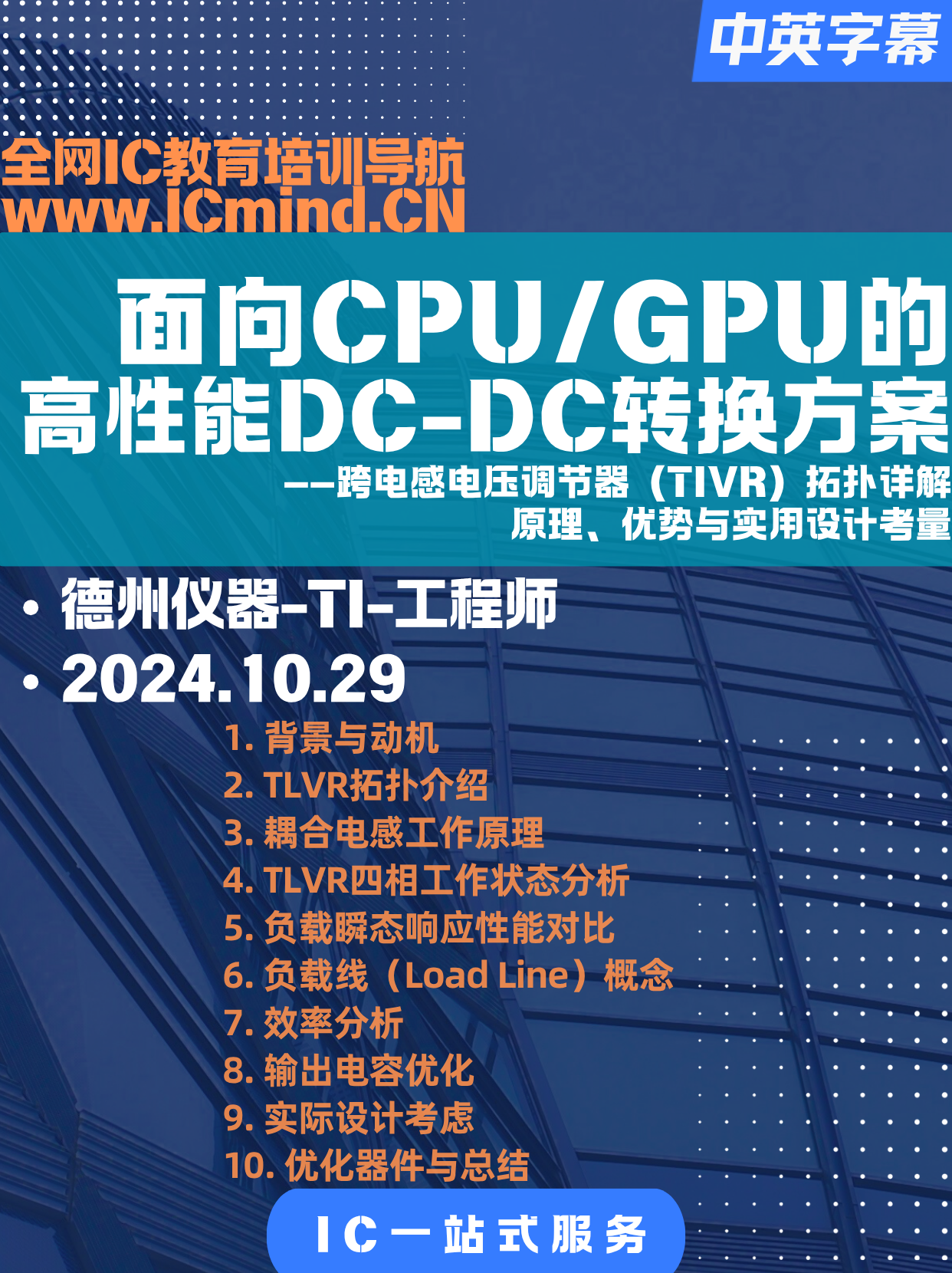
TI-面向CPU/GPU的高性能DC-DC转换方案:跨电感电压调节器(TIVR)拓扑详解
TI-面向CPU/GPU的高性能DC-DC转换方案:跨电感电压调节器(TIVR)拓扑详解
1. 背景与动机 2. TLVR拓扑介绍 3. 耦合电感工作原理 4. TLVR四相工作状态分析 5. 负载瞬态响应性能对比 6. 负载线(Load Line)概念 7. 效率分析 8. 输出电容优化 9. 实际设计考虑 10. 优化器件与总结
完整版私信客服 186-6709-0885
![[2024]垂直供电-突破xPU与AI算力瓶颈的必然之路-ADI收购Empower](https://material-image.wanwang.xin/1597234105050516/public/ead0ee54-ca02-45bc-acf5-550c2d45948d.png)
[2024]垂直供电-突破xPU与AI算力瓶颈的必然之路-ADI收购Empower
[2024]垂直供电-突破xPU与AI算力瓶颈的必然之路-ADI收购Empower
大纲 PCB正成为算力“水管瓶颈” 传统供电拓扑的固有问题 瞬态响应与算力损失的关联 垂直供电的解决方案 附加收益与密度优势 代价:散热与空间约束 Q&A与总结
完整版私信客服 186-6709-0885
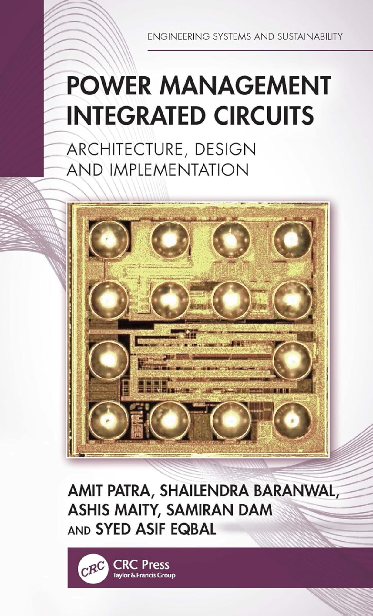
【教材】Power Management Integrated Circuits Architecture, Design and Implementation ( etc.)
【教材】Power Management Integrated Circuits Architecture, Design and Implementation ( etc.)
本书旨在成为一本关于电源管理集成电路的综合性教材,将理论基础和实践细节相结合,为研究和工业领域提供成功的设计实践。本书涵盖了电源管理电路的三大主要类别,即线性稳压器、基于电感的开关转换器和开关电容电路,并详细讨论了它们常见的拓扑结构、工作原理和建模方法。 特性 包括电源管理集成电路(PMIC)的基础理论和设计/实现实用要素。 提供与线性稳压器、开关电容转换器和基于电感的转换器相关的拓扑结构和电路的深入分析。 涵盖电力电子与集成电路设计领域交叉处的所有相关主题。 为电路设计提供指导方针,并为所有相关拓扑提供解决方案。 指出电源管理集成电路(PMIC)设计中所有重要问题及相关权衡。 这本书对于高年级学生、研究生以及修过模拟电路设计、控制系统和电力电子大学课程的行业专业人士来说,将是一本宝贵的资源。
完整版私信客服 186-6709-0885
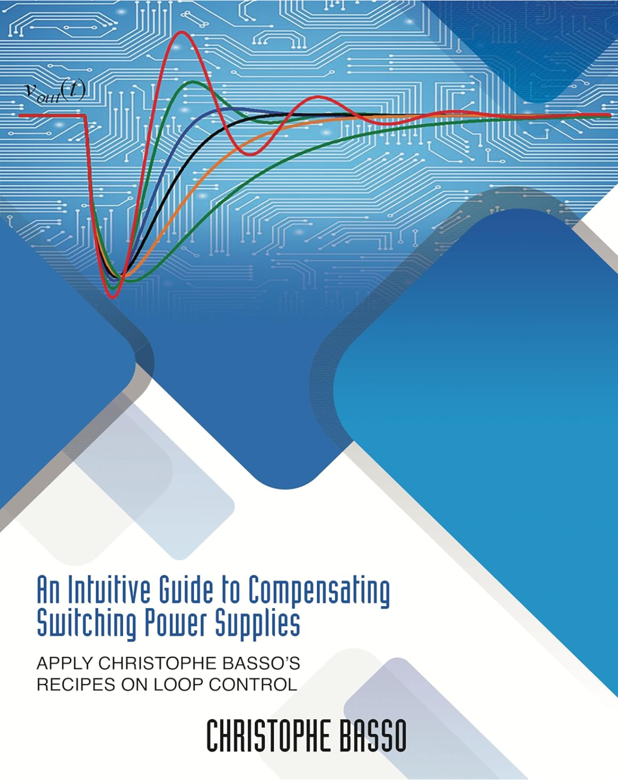
【教材】An Intuitive Guide to Compensating Switching Power Supplies: Apply Christophe Basso’s Recipes on Loop Control
【教材】An Intuitive Guide to Compensating Switching Power Supplies: Apply Christophe Basso’s Recipes on Loop Control
《开关电源补偿直观指南》是一本面向电源工程师的实用手册,旨在帮助工程师们设计出稳定且可靠的转换器。大多数涉及环路控制的技术书籍都深入理论,但在设计方面却浅尝辄止,缺乏实际示例。 这本新书介绍了直观的理论——好消息是,在控制回路方面,你不需要了解所有知识也能做好工作——然后深入讲解了许多使用SIMPLIS®模拟的示例。所有示例均可免费下载,且大多数示例可在Elements演示版上运行。安装Elements后,你就可以开始模拟你的转换器了! 本书内容包括: ▪ 几页理论内容。.. ▪ 电压模式控制下的降压转换器 ▪ 电流模式控制下的降压转换器 ▪ 电压模式控制下的正激变换器 ▪ 各种控制方案中的LLC转换器 ▪ 还有更多关于PFC和UC384x电路的示例 通过阅读本书,你将不再随意选择交叉频率或相位裕度。你将学会如何使用运算放大器、TL431或OTA(运算跨导放大器)通过补偿器来提升相位,同时也会了解光耦如何降低相位裕度。我详细介绍了扩展带宽的选项,以及更多技巧,旨在使读者成为环路补偿方面的专家。 这本书不仅是研究生和经验丰富的工程师的理想读物,对于那些希望深入了解该主题并在客户遇到问题时提供帮助的现场应用工程师(FAE)来说,也是一本不可或缺的指南。
完整版私信客服 186-6709-0885
![[PLL]清华大学-李宇根教授-PLL锁相环设计实战课程- 20年产业经验分享](https://material-image.wanwang.xin/1597234105050516/public/363660fc-7fcd-4475-bbc7-c57fa733bd6a.png)
[PLL]清华大学-李宇根教授-PLL锁相环设计实战课程- 20年产业经验分享
[PLL]清华大学-李宇根教授-PLL锁相环设计实战课程- 20年产业经验分享
本视频专访清华大学集成电路学院教授李宇根,他拥有10年美国产业界经验(Conexant、IBM Watson研究中心)和18年中国学术界经验,曾设计量产超2000万颗芯片的GSM射频收发机。吴刚教授详细介绍其即将开设的PLL锁相环设计课程,涵盖系统视角、电路设计实践、先进架构与未来挑战四大模块,适合有经验的混合信号电路设计师、产业工程师及学术研究人员。课程将结合真实设计案例与量产经验,传授从系统需求分析到鲁棒性设计的完整方法论。
完整版私信客服 186-6709-0885
![[PLL]清华大学-李宇根教授-锁相环(PLL)设计与分析全览:系统、电路、架构及高级技术](https://material-image.wanwang.xin/1597234105050516/public/33a5cd02-deda-4fd7-a3b0-70af66b1fdff.png)
[PLL]清华大学-李宇根教授-锁相环(PLL)设计与分析全览:系统、电路、架构及高级技术
[PLL]清华大学-李宇根教授-锁相环(PLL)设计与分析全览:系统、电路、架构及高级技术
本视频预览围绕锁相环(PLL)设计展开,涵盖系统级分析、电路设计、架构选择及高级PLL技术四大核心板块。内容包括时钟抖动的频域分析与预算规划、时钟生成与频率产生的关键指标(如时序余量、频谱纯度),并通过案例研究深入探讨设计问题。电路设计部分聚焦鉴相器(PFD)、CML分频器、压控振荡器(VCO)等关键模块的设计挑战与优化策略。架构方面则对比分析整数N型PLL、小数N型PLL、全数字PLL(DPLL)及混合PLL,强调低电源电压下的性能提升与噪声优化,为PLL设计者提供从基础到高级的全面技术预览。
完整版私信客服 186-6709-0885
![[PLL]清华-李宇根-PLL分频器产品级设计思路](https://material-image.wanwang.xin/1597234105050516/public/1cdddd54-e8a4-4183-b3b1-a0ce5a3fe3f9.png)
[PLL]清华-李宇根-PLL分频器产品级设计思路
[PLL]清华-李宇根-PLL分频器产品级设计思路
本文主要围绕产品级设计中分频器的选择与设计展开,重点分析了动态逻辑分频器的不足,强烈建议采用电流模式逻辑(CML)分频器,并详细阐述了CML分频器设计中的关键参数、输入缓冲、功耗权衡、版图布局等核心要点及优化策略,以确保其在实际产品中的可靠性和性能。
完整版私信客服 186-6709-0885
![[PLL]清华大学-李宇根教授-电荷泵电流失配问题分析与计算](https://material-image.wanwang.xin/1597234105050516/public/91e3d925-e6b2-447d-ac8e-b867c76058eb.png)
[PLL]清华大学-李宇根教授-电荷泵电流失配问题分析与计算
[PLL]清华大学-李宇根教授-电荷泵电流失配问题分析与计算
简介:本文围绕电荷泵电流失配的最大允许值展开讨论,结合给定的环路参数(如参考频率、PFD最小翻转时间、电荷泵电流、RC元件值、VCO增益等),通过计算单位增益频率、零点频率、极点频率及相位裕度,基于 lecture 笔记中的简化模型,最终得出为满足10-60dbc参考要求,电荷泵上下电流源的最大失配需小于8%。
完整版私信客服 186-6709-0885
【教材】Advanced DC-DC Power Converters and Switching Converters II
【教材】Advanced DC-DC Power Converters and Switching Converters II
近年来,市场对性能提升(如低能耗和尺寸减小)的电源转换器的需求日益强烈。新兴应用,如电动汽车(牵引逆变器、车载DC-DC充电器、DC-DC电池转换器等)、数据中心电源管理(UPS和总线转换器)、变速驱动器、智能电网的低压/高压转换器接口以及能源转换(可再生能源开关电源转换器接口和电池储能转换器)推动了这一改进趋势。效率和功率密度是管理先进电源转换器应用的关键参数。特刊“先进DC-DC电源转换器和开关转换器II”重点关注新兴电力电子应用战略领域中开关电源转换器的先进解决方案,以促进技术发展。文章通过描述先进开关转换器在能源转换中的创新解决方案,为这些领域做出了贡献,这些解决方案致力于在现代社会发展中使用可持续技术。
完整版私信客服 186-6709-0885
【课程】均衡器 Equalizers 台大 李致毅老师
【课程】均衡器 Equalizers 台大 李致毅老师
本系列课程系统讲解高速有线通信(SerDes)系统中的信号完整性恢复技术,是芯片设计工程师与通信系统开发者深入理解均衡器(Equalizer)架构的完整指南。 课程从宽带电路与高速数据传输的基础出发,深入剖析有线信道中的信号损伤机制,包括趋肤效应、介质损耗导致的幅度衰减,以及阻抗不匹配引发的反射与码间干扰(ISI)。通过对信道冲激响应、主光标/前光标/后光标(Main/Precursor/Post cursor)及眼图闭合的量化分析,建立对通道特性的系统认知。 在此基础上,课程逐一详解三大主流均衡器架构: 前馈均衡器(FFE):从FIR滤波器原理、多抽头零强迫(Zero Forcing)系数优化,到全速/半速电路实现、电流合并架构与高速设计挑战; 连续时间线性均衡器(CTLE):涵盖差分对源极退化电路设计、零点极点配置、多级级联与电感峰值技术,并深入探讨基于Slicer的功率检测自适应方案及无需Slicer的频谱能量自适应方法; 判决反馈均衡器(DFE):从IIR模型与稳定性判据出发,详解多抽头系数确定、高速CML电路实现、动态阈值调整,以及针对时序瓶颈的推测(Speculation)与亚速率(Sub-rate)架构优化。 最后,课程还涵盖DFE的自适应算法实现,包括资源受限环境下的Sign LMS算法,以及面向PAM4等多电平信号的改进型电平跟踪与参考电平自适应技术,为高速IO接收端设计提供从理论到工程实践的全链路支撑。 关键词 高速SerDes、信号完整性、均衡器(Equalizer)、前馈均衡器(FFE)、连续时间线性均衡器(CTLE)、判决反馈均衡器(DFE)、信道损耗、码间干扰(ISI)、趋肤效应、介质损耗、反射、阻抗匹配、眼图、奈奎斯特频率、零强迫(Zero Forcing)、抽头系数、FIR滤波器、IIR滤波器、源极退化、电感峰值、自适应均衡(Adaptation)、Sign LMS算法、PAM4、电平跟踪、Slicer、半速架构(Half-Rate)、推测技术(Speculation)、高速IO、有线通信、宽带电路
完整版私信客服 186-6709-0885
2024峰值电流模式(PCM)控制:原理、次谐波振荡与内环增益揭秘
2024峰值电流模式(PCM)控制:原理、次谐波振荡与内环增益揭秘
引言与背景 峰值电流模式(PCM)控制基础 系统级构成与外环控制 稳定性难题:次谐波振荡 标准解决方案:斜率补偿 仿真演示与关键波形观察 核心揭秘:内环增益测量 尾声:对AI(ChatGPT)回答的思考
完整版私信客服 186-6709-0885
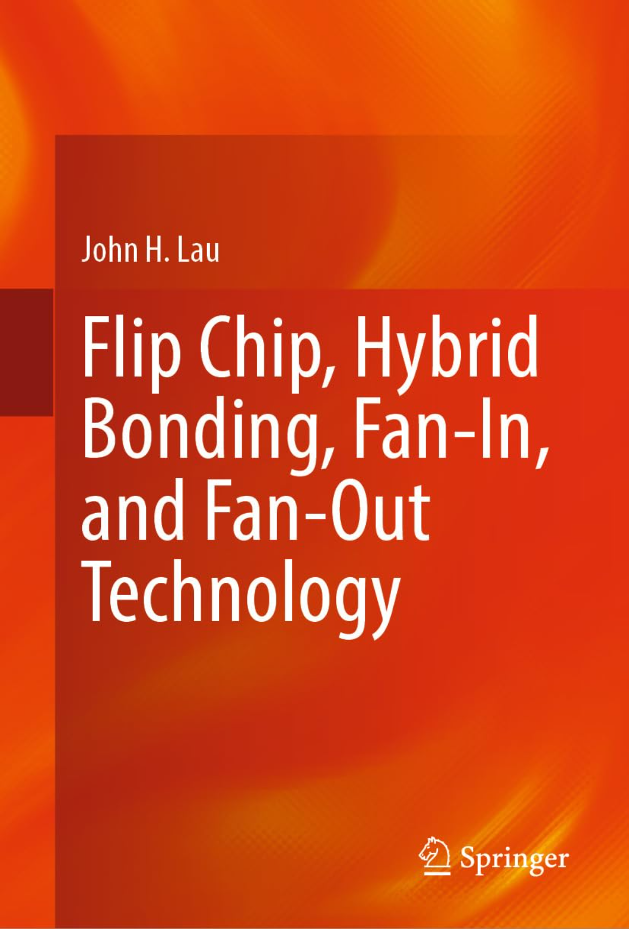
【教材】Flip Chip, Hybrid Bonding, Fan-In, and Fan-Out Technology
【教材】Flip Chip, Hybrid Bonding, Fan-In, and Fan-Out Technology
本书重点介绍倒装芯片、混合键合、扇入和扇出技术的设计、材料、工艺、制造和可靠性。既涉及原理,也涉及工程实践,但更侧重于工程实践。通过深入研究多个主要课题,如晶圆凸点、倒装芯片组装、底部填充和可靠性、芯片到晶圆、晶圆到晶圆、铜-铜混合键合、WLCSP、六面模塑WLCSP、FOWLP(如带PID的混合基板、ABF和超大型有机中介层)、小芯片与异构集成封装之间的通信,以及板上光学器件、近封装光学器件和共封装光学器件,实现了这一目标。 这本书对电气工程、机械工程、材料科学、工业工程等领域的研究人员、工程师和研究生大有裨益。
完整版私信客服 186-6709-0885
[2024-ISSCC-Plenary Session]-《半导体行业未来十年:AI驱动的万亿美元机遇与创业创新》
[2024-ISSCC-Plenary Session]-《半导体行业未来十年:AI驱动的万亿美元机遇与创业创新》
华登国际创始人兼董事长Lip-Bu Tan在ISSCC2024会议的压轴演讲中,结合其40年风险投资生涯洞察,系统阐述了人工智能时代半导体行业的五大驱动力(数据中心、自动驾驶、工业物联网、5G/6G通信及可持续气候技术),并分享了万亿美元市场机遇、技术变革趋势、创业投资心得、前沿布局方向及行业人才培养等核心内容,为工程师、创业者和投资者提供了详实的行业路线图。
完整版私信客服 186-6709-0885
![[IA]仪表放大器原理详解:高精度差分放大器的设计与优势分析-新加坡国立大学](https://material-image.wanwang.xin/1597234105050516/public/139de394-1daa-40e8-b06a-21ae10e56475.png)
[IA]仪表放大器原理详解:高精度差分放大器的设计与优势分析-新加坡国立大学
[IA]仪表放大器原理详解:高精度差分放大器的设计与优势分析-新加坡国立大学
本视频深入讲解仪表放大器(Instrumentation Amplifier)的工作原理与设计优势。作为高精度差分放大器,仪表放大器在理想情况下共模增益为零,实际应用中也非常接近零。视频首先回顾了简单差分放大器的三大缺陷:输入阻抗较低、增益调节困难、共模增益依赖电阻匹配精度。随后通过逐步改进的方式,展示了如何通过添加缓冲级和采用两级结构来克服这些缺陷。重点推导了仪表放大器的差分增益公式(1+2R₂/R₁),分析了共模增益为1的第一级如何与差分放大器第二级配合,实现整体零共模增益。最后总结了仪表放大器的核心优势:高输入阻抗、高共模抑制比(CMRR)以及通过单一电阻(R₁)即可调节增益的便利性。
完整版私信客服 186-6709-0885
【课程】2T的无BJT电压基准源
【课程】2T的无BJT电压基准源
超低功耗,两个MOS实现(需要nativeMOS)
完整版私信客服 186-6709-0885
【教材】PLL Modulation and Mixed-Signal Calibration Techniques for FMCW Radar
【教材】PLL Modulation and Mixed-Signal Calibration Techniques for FMCW Radar
本书涵盖了现代FMCW雷达炉膛中使用的基于PLL的频率调制器的分析和设计。首先,将所需的雷达性能目标转化为调制器规格。然后,作者重点描述了最佳调制器架构,特别关注了系统的核心构建块。所描述的中央模拟构建块是一种基于电荷积分的新型啁啾发生器,它打破了性能(噪声、面积)受限领域类似技术的限制。。。
完整版私信客服 186-6709-0885
【教材】孙楠-现代模拟集成电路设计
【教材】孙楠-现代模拟集成电路设计
内有40nm的gm/id设计运放的详细推导过程;"讲解简单易懂,注重直觉理解;围绕先进工艺节点介绍现代模拟集成电路分析与设计方法; 包含大量设计实例 "。
完整版私信客服 186-6709-0885
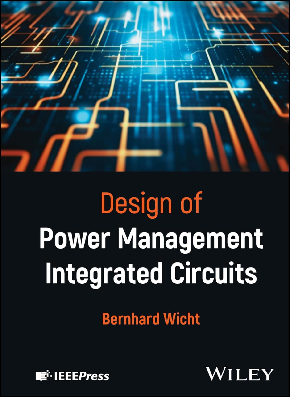
【教材】Design of Power Management Integrated Circuits (IEEE Press) 1st Edition
【教材】Design of Power Management Integrated Circuits (IEEE Press) 1st Edition
电源管理集成电路设计
完整版私信客服 186-6709-0885
【教材】Advances in Photonics and Electronics
【教材】Advances in Photonics and Electronics
对光子学和电子学的最新进展进行了全面综述 强调基于应用的创新 面向光电子领域的学生、研究人员、教授和行业专业人士
完整版私信客服 186-6709-0885
【教材】Advanced CMOS Biochips: Design and Fabrication (Analog Circuits and Signal Processing)
【教材】Advanced CMOS Biochips: Design and Fabrication (Analog Circuits and Signal Processing)
生物芯片整合了多种手段,包括电子、光子和微流体器件;生物材料(活细胞、组织、酶、核酸等)以及化学分析,以产生可检测的信号来识别生物现象。在几种相互竞争的生物芯片技术中,互补金属氧化物半导体(CMOS)工艺具有成本低、集成化、高精度和便携的优势,适用于即时诊断。 先进CMOS生物芯片采用多路径方法:生物界面的微电子设计与实现,为电气、磁、光学和机械传感及驱动模块等广泛的集成电路和系统提供了重要的当代视角;生物学、生物化学以及微流体学的经典知识。其内容既实用又深入,整合了实验、理论和模拟示例。通过使用先进CMOS生物芯片,读者将掌握基本原理和设计技术,以应对CMOS生物芯片器件中通常出现的情况。
完整版私信客服 186-6709-0885
【教材】Co-simulations of Microwave Circuits and High-Frequency Electromagnetic Fields
【教材】Co-simulations of Microwave Circuits and High-Frequency Electromagnetic Fields
本书旨在以先进设计系统(ADS)和高频结构模拟器(HFSS)为仿真平台,提供微波电路和高频电磁(EM)场的诸多高级应用主题。特别是,它包含了有关元器件和设备设计的最新多学科协同仿真指导。目前,电路/场设计以及性能分析与优化在很大程度上依赖于各种功能强大的电子设计自动化(EDA)软件。射频/微波工程师必须掌握两种或更多相关的仿真设计软件。是德科技的ADS和安捷伦的HFSS分别是电路仿真以及微波器件场和结构仿真的代表。目前,这两类软件在企业、大学和研究机构中得到广泛应用。本书的主要目的是让对微波工程和应用电磁学感兴趣的读者掌握这两种工具的应用。它还帮助读者拓展这些软件背后的知识边界,并通过协同仿真加深对跨学科技术发展的理解。 本书分为三个部分。第一部分介绍ADS和HFSS的两个最新版本,帮助读者更好地理解基本原理和最新功能,并就如何为不同问题选择合适的仿真工具提供建议。第二部分主要介绍高频电磁场、微波电路、天线设计、电磁兼容性(EMC)以及热和结构分析的协同仿真。它分别提供了将ADS和HFSS与其他类型软件结合进行协同仿真的指导和建议。最后一部分讲述协同仿真的自动化接口和脚本编程方法。它主要涉及ADS中的高级扩展语言(AEL)、Python数据链接(PDL)和MATLAB接口。对于HFSS,它讨论了VBScript、IronPython脚本以及基于MATLAB的应用程序编程接口(API)。每个主题都包含实用示例,以帮助读者理解,使他们能够获得基于这些软件的自动化接口和脚本编程方法的扎实知识和技能。 本书结合实例编写简洁,非常适合作为微波电路和电磁仿真入门课程的教材,也可作为电子学、微波工程、通信工程及相关领域许多课程的补充教材。同时,它也可作为微波工程师和研究人员的参考书。
完整版私信客服 186-6709-0885
【教材】Mixed-Signal CMOS for Wireline Communication: Transistor-Level and System-Level Design Considerations
【教材】Mixed-Signal CMOS for Wireline Communication: Transistor-Level and System-Level Design Considerations
通过作者在工业和学术环境中开发PMIC的经验,《电源管理集成电路设计》一书为这一快速发展的技术提供了独特见解,其中包括以下内容:
完整版私信客服 186-6709-0885
[IA]仪表放大器原理详解:高精度差分放大器的设计与优势分析
[IA]仪表放大器原理详解:高精度差分放大器的设计与优势分析
视频标题 仪表放大器原理详解:高精度差分放大器的设计与优势分析 --- 视频简介 本视频深入讲解仪表放大器(Instrumentation Amplifier)的工作原理与设计优势。作为高精度差分放大器,仪表放大器在理想情况下共模增益为零,实际应用中也非常接近零。视频首先回顾了简单差分放大器的三大缺陷:输入阻抗较低、增益调节困难、共模增益依赖电阻匹配精度。随后通过逐步改进的方式,展示了如何通过添加缓冲级和采用两级结构来克服这些缺陷。重点推导了仪表放大器的差分增益公式(1+2R₂/R₁),分析了共模增益为1的第一级如何与差分放大器第二级配合,实现整体零共模增益。最后总结了仪表放大器的核心优势:高输入阻抗、高共模抑制比(CMRR)以及通过单一电阻(R₁)即可调节增益的便利性。 --- 关键词 仪表放大器、差分放大器、运算放大器、共模增益、差分增益、共模抑制比、CMRR、输入阻抗、电压跟随器、缓冲器、电阻匹配、增益调节、两级放大器、精密测量、传感器信号调理
完整版私信客服 186-6709-0885
【教材】Design of Power Management Integrated Circuits (IEEE Press) 1st Edition
【教材】Design of Power Management Integrated Circuits (IEEE Press) 1st Edition
《电源管理集成电路设计》是一本全面的电源管理集成电路(IC)设计参考书,涵盖了线性稳压器和开关式稳压器等主要电源管理电路的电路设计,以及电源开关、门驱动器及其供电、电平转换器、误差放大器、电流检测和控制回路设计等子电路。该书还介绍了保护和诊断电路,以及横向和纵向电源输送、引脚布局、平面规划、接地/供电指南和封装等物理设计方面。书中专门用一章来介绍集成无源器件的设计。本书阐述了电源管理集成电路(PMIC)在计算、物联网、移动通信和可再生能源等增长领域的应用。 包含众多真实世界的示例、案例研究和练习,以阐释关键的设计概念和技巧。
完整版私信客服 186-6709-0885
【教材】Integrated Electronic Circuits
【教材】Integrated Electronic Circuits
为电子电路基础课程提供易于理解且最新的内容 涵盖模拟、数字和混合信号电路以及应用和技术方面 强调使用EDA工具进行集成电路设计,并提供丰富的在线资源
完整版私信客服 186-6709-0885
【教材】Integrated Circuit Fabrication: Science and Technology
【教材】Integrated Circuit Fabrication: Science and Technology
通过这本权威教材,掌握现代半导体集成电路的基础技术。它首先介绍了最先进的CMOS工艺流程,从一开始就让学生接触全局思维,并鼓励他们培养实用的集成思维。通过大量使用Silvaco Athena和Victory Process等行业工具进行工艺和TCAD模拟,使学生更深入地了解物理原理,并为他们在现实环境中应用这些工具做好准备。本书采用易于理解的框架,仅假设学生具备基本的化学、物理和数学背景,为来自不同背景的学生提供了循序渐进的介绍;书中包含450多幅插图(许多为彩色插图)和280多个章节末尾的问题,将支持和巩固学生的理解。本书配有授课幻灯片和教师解决方案,是电气工程、材料科学和物理学高年级本科生和研究生以及寻求权威入门参考的半导体工程专业人士学习半导体技术的理想入门教材。
完整版私信客服 186-6709-0885
【课程】PLL 台大 李致毅老师
【课程】PLL 台大 李致毅老师
深入浅出的介绍了PLL;个人主页:李致毅教授的簡傳 - Biography of Jri Lee
完整版私信客服 186-6709-0885
UC伯克利:1200A/1V开关总线转换器解析
UC伯克利:1200A/1V开关总线转换器解析
简介 AI算力爆发式增长,GPU功耗十年暴涨10倍!传统供电架构面临巨大挑战。加州大学伯克利分校的最新研究,提出了一种全新的**48V直降1V单级开关总线转换器(Switching Bus Converter)**,能以**1200安培**的惊人电流为下一代超高性能微处理器供电。 这项技术通过创新的拓扑融合与架构设计,不仅实现了**92.4%的峰值效率**和**87.5%的满载效率**,更达到了**67瓦/立方英寸**的超高功率密度,性能远超现有方案。视频将深入浅出地为你讲解: - 为何传统“两级”供电架构已不堪重负? - “开关总线”架构相比“直流总线”的三大核心优势。 - 如何一步步推导出这款复杂的混合式开关电容转换器拓扑。 - 硬件原型设计细节与实测性能数据解析。 - 与NVIDIA合作的下一代原型方向。 如果你对GPU供电、数据中心基础设施、高功率密度电源设计感兴趣,这期干货不容错过!
完整版私信客服 186-6709-0885
【课程】天津大学-聂老师-BG综述
【课程】天津大学-聂老师-BG综述
BG综述,一阶详细讲解+高阶补偿部分引入
完整版私信客服 186-6709-0885

芯片内部去耦技术:从原理到实测的EMI优化方案
芯片内部去耦技术:从原理到实测的EMI优化方案
本视频深入讲解集成电路中的片上去耦(On-Chip Decoupling,OCD)技术。从传统外部去耦电容的局限性出发,详细介绍如何将去耦电容集成到芯片内部,包括键合线、金属环、电源轨等寄生参数的影响分析。重点探讨了栅极电容作为片上去耦元件的优势与ESD防护挑战,并展示了一种创新的交叉保护晶体管结构。通过实际测试芯片的对比实验,验证了片上去耦可使电磁发射降低约14dB。最后讨论了盲目填充空闲区域策略的潜在问题,提出了战略性布局与阻尼电阻配合的优化方向。
完整版私信客服 186-6709-0885
IEEE-研讨会-印度-01-高速串行技术测量挑战深度解析:从PCIe 6.0 PAM4、USB4到DDR5的物理层测试与合规验证
IEEE-研讨会-印度-01-高速串行技术测量挑战深度解析:从PCIe 6.0 PAM4、USB4到DDR5的物理层测试与合规验证
本视频为泰克资深专家Naresh关于高速串行技术测试测量的深度技术分享。随着数据传输速率呈指数级增长,物理层测试正面临前所未有的挑战。讲座系统梳理了当前主流高速接口技术的演进与测试痛点,包括PCI Express、USB4、DDR5/DDR6等,并完整覆盖了高速测试的核心方法论,为芯片验证、板级调试或合规认证等提供从标准解读到工程实践的系统性指导。
完整版私信客服 186-6709-0885
【IC通识内容】【讲座】赋能科研与学习之旅
【IC通识内容】【讲座】赋能科研与学习之旅
拉神,无需多言了
完整版私信客服 186-6709-0885
【教材】Chiplet Design and Heterogeneous Integration Packaging
【教材】Chiplet Design and Heterogeneous Integration Packaging
本书聚焦于小芯片设计和异构集成封装的设计、材料、工艺、制造和可靠性。既涵盖了原理,也涉及了工程实践,且更侧重于工程实践。通过深入研究多个重要主题,如芯片划分、芯片分割、采用TSV(硅通孔)中介层的多个系统和异构集成、采用无TSV中介层的多个系统和异构集成、小芯片横向通信、系统级封装、扇出晶圆/面板级封装以及各种铜-铜混合键合技术,实现了这一目标。本书对电气工程、机械工程、材料科学和工业工程等领域的研究人员、工程师和研究生均有益处。
完整版私信客服 186-6709-0885
【课程】天津大学-聂老师-全差分运放噪声分析
【课程】天津大学-聂老师-全差分运放噪声分析
逐步推导,详细明了;
完整版私信客服 186-6709-0885
[2023-ISSCC-Plenary Session]高性能计算的未来与Zeta级挑战-AMD CEO苏姿丰ISSCC 2023主题演讲:
[2023-ISSCC-Plenary Session]高性能计算的未来与Zeta级挑战-AMD CEO苏姿丰ISSCC 2023主题演讲:
AMD董事长兼CEO苏姿丰博士在国际固态电路会议(ISSCC)2023上发表主题演讲,回顾ISSCC成立70周年及半导体行业进步。演讲重点探讨高性能计算(HPC)发展趋势、人工智能对算力的需求,以及实现Zeta级计算(比现有百亿亿次级快1000倍)面临的核心挑战——能源效率。苏姿丰详细介绍了AMD在先进封装、3D堆叠、Chiplet架构、存算一体等领域的创新实践,并展望了AI与HPC融合、光电共封装等前沿方向,呼吁全行业跨学科协作突破物理极限。
完整版私信客服 186-6709-0885
![[DCDC]多相BUCK-跨电感稳压器TLVR直观解读](https://material-image.wanwang.xin/1597234105050516/public/5b7a2182-9223-4cea-8720-b22fdce758a8.png)
[DCDC]多相BUCK-跨电感稳压器TLVR直观解读
[DCDC]多相BUCK-跨电感稳压器TLVR直观解读
背景与问题引入 传统多相Buck转换器 TLVR拓扑结构概述 TLVR工作原理的直观分析 负载瞬态响应的仿真对比 公平比较与工程考量
完整版私信客服 186-6709-0885
【课程】东南大学吴金老师的基准部分
【课程】东南大学吴金老师的基准部分
东南大学吴金老师的2013年录课;原理通俗易懂
完整版私信客服 186-6709-0885
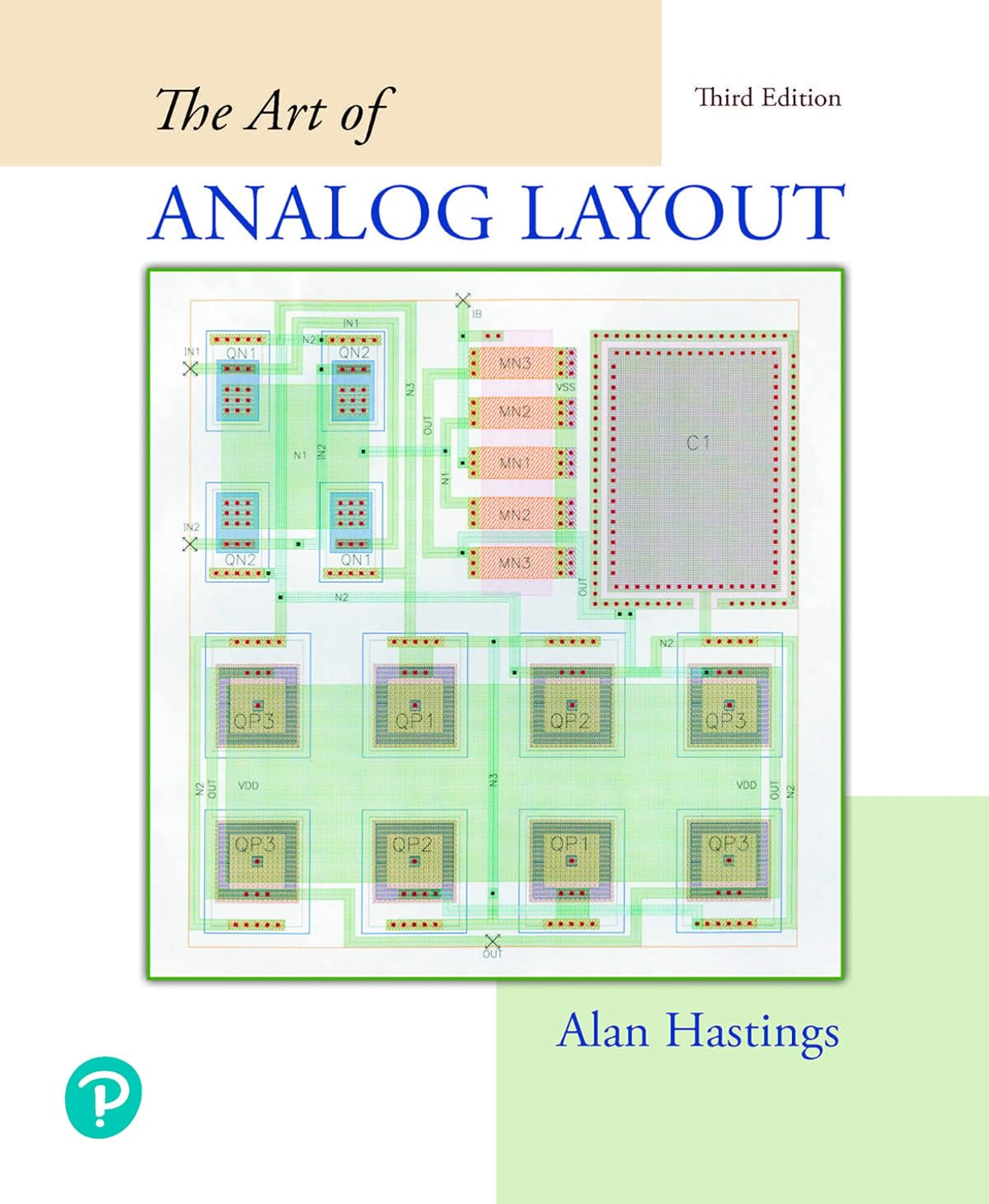
【教材】Art of Analog Layout, The 3rd Edition
【教材】Art of Analog Layout, The 3rd Edition
《模拟版图的艺术》涵盖了成功设计模拟集成电路版图所涉及的问题。它提供了清晰的指导,并以易于理解的方式呈现材料,既不牺牲细节,也不会用版图的理论物理或数学分析让你感到晦涩难懂。与更常见的器件几何和 schematic 表示相比,本书重点介绍了器件的横截面和基于载流子的器件工作模型。 第三版经过全面重写,以反映该领域的变化,包括新增了一章关于版图的内容,以及关于失效机制、电阻器、电容器和电感器、双极晶体管及其应用、MOS 晶体管等方面的新内容。
完整版私信客服 186-6709-0885
【教材】High-Performance and High-Speed Pipelined ADCs
【教材】High-Performance and High-Speed Pipelined ADCs
本书讨论了有效设计高速(多GS/s)和高性能流水线ADC所需的理论基础和设计技术,这些ADC在各种系统的信号链中起着关键作用。读者将逐步了解流水线ADC及其拓扑结构的设计和分析,并学习理论和实践设计细节,从而能够探索和构建这些数据转换器。作者还详细介绍了流水线ADC的各个方面及其对ADC速度和性能的影响,重点关注输入缓冲器和采样网络、基准放大器、比较器及其对ADC错误率和高频性能的影响,以及失配估计和校正。
完整版私信客服 186-6709-0885
【教材】High-Speed System and Analog Input/Output Design
【教材】High-Speed System and Analog Input/Output Design
本教材新版基于 Thanh T. Tran 博士在莱斯大学教授高速数字和模拟设计课程 10 余年的经验,以及其在高速系统设计领域 30 余年的工作经验,包括数字信号处理(DSP)、计算机和嵌入式系统中的信号与电源完整性。本书为学生和在职工程师提供高速数字和模拟设计的实践操作指导。作者首先介绍了良好的高速数字和模拟设计实践,这些实践可最大限度地减少元件和系统噪声,确保系统设计成功。然后,他提出了在整个设计过程中应遵循的准则,以减少噪声和辐射,避免常见陷阱,同时提高质量和可靠性。书中充满了关于设计和系统仿真的技巧,可最大限度地降低后期重新设计成本和产品发货延迟。全书重点介绍了音频、视频、模拟滤波器、DDR 内存和电源的实践设计示例。此外,作者还提供了一种实用方法来设计多吉赫兹高速串行总线(USB-C、PCIe、HDMI、DP),并使用 S 参数模型仿真印刷电路板的插入损耗和回波损耗。
完整版私信客服 186-6709-0885
【教材】Multi-Gigahertz Nyquist Analog-to-Digital Converters
【教材】Multi-Gigahertz Nyquist Analog-to-Digital Converters
本书提出了在深亚微米CMOS和FinFET技术中的创新电路、架构和系统解决方案,旨在解决最大化多GHz采样率和带宽模数转换器(ADC)的精度*速度/功率方面的挑战。书中引入了一种新的整体方法,该方法首先识别转换器构建模块的主要误差源,并定量分析它们对整体性能的影响,确立了电路施加的基本精度-速度-功率限制。分析扩展到架构层面,通过引入数学框架来估计和比较多种ADC架构及其变体的精度-速度-功率限制。为了获得系统级洞察,详细介绍了时间交织技术,并引入了一个框架来定量比较交织器架构的关键指标。还通过添加几种深亚微米CMOS技术的工艺效应来考虑技术的影响。 所引入的分析方法的有效性和所提出概念的可行性通过四个硅原型集成电路(IC)得到了证明,这些原型在超深亚微米CMOS和FinFET技术中实现。 引入了一种新的整体方法,用于深亚微米CMOS技术中高性能ADC的分析和设计,从理论概念到硅片实现和验证; 描述了推动多GHz ADC精度-速度-功率边界的新方法和技术,分析了整个ADC链中核心和外围电路的权衡; 通过四个采用28nm体CMOS和16nm FinFET技术实现的最先进硅原型IC支持所引入的分析和设计概念; 为ADC设计初学者和经验丰富的工程师提供了有用的参考和宝贵的工具。
完整版私信客服 186-6709-0885
【教材】 The Art of Analog Layout_3
【教材】 The Art of Analog Layout_3
常用的电平转换器(包括尺寸规则)以及级联(锥形)驱动器的尺寸确定和优化指南
完整版私信客服 186-6709-0885
[SerDes]高速SerDes中为什么需要Mueller-Muller CDR?与Bang-Bang CDR的全面对比
[SerDes]高速SerDes中为什么需要Mueller-Muller CDR?与Bang-Bang CDR的全面对比
本视频深入探讨了在高速串行接口(SerDes)设计中,为何越来越多的系统选择Mueller-Muller时钟数据恢复(CDR)替代传统的Bang-Bang CDR。内容涵盖Bang-Bang CDR的基本原理及其在高速传输中的局限性,包括2倍过采样带来的功耗、时钟相位失配等挑战。视频进一步分析了在PAM4调制和ADC-based架构下,Mueller-Muller CDR如何通过波特率采样(每单位间隔一次采样)优化系统性能,并利用信道脉冲响应的对称性实现更稳健的时钟恢复。适合高速电路设计、通信系统及芯片开发领域的工程师和研究人员观看,帮助理解CDR技术演进及其在下一代SerDes中的应用趋势。
完整版私信客服 186-6709-0885
【课程】LDO-nksunmoon-基本工作原理
【课程】LDO-nksunmoon-基本工作原理
系统地介绍了LDO的功能、结构、工作原理、关键参数以及稳定性分析
完整版私信客服 186-6709-0885
![IEEE-研讨会-印度-04-[SerDes]高速有线通信电路与系统挑战:从LVDS到PAM4及3D IC封装互联技术](https://material-image.wanwang.xin/1597234105050516/public/4dc87a0e-7bf0-46cf-9665-cb7e42e6c885.png)
IEEE-研讨会-印度-04-[SerDes]高速有线通信电路与系统挑战:从LVDS到PAM4及3D IC封装互联技术
IEEE-研讨会-印度-04-[SerDes]高速有线通信电路与系统挑战:从LVDS到PAM4及3D IC封装互联技术
本视频由Intel Bangalore资深模拟/混合信号工程师Tapas主讲,系统介绍高速有线通信(Wireline Communication)电路与系统面临的核心挑战及解决方案。 讲座内容涵盖: 基础技术演进 - LVDS(低压差分信号):差分传输原理、电流源驱动、接收端差分放大器与Strong Arm锁存器 - 源同步系统(Source Synchronous):时钟前向传输、串并/并串转换、眼图与单位间隔(UI)概念 时钟与数据恢复(CDR) - 抖动(Jitter)分类:确定性抖动与随机抖动、误码率(BER)概念 - 延迟锁定环(DLL)与相位插值器(Phase Interpolator) - Alexander/Bang-Bang相位检测器原理 - CDR类型对比:盲过采样、模拟PLL型、数字DCO/相位旋转器型 信道均衡技术 - CTLE(连续时间线性均衡器):源退化差分放大器、零点与极点设计 - FFE(前馈均衡器):预失真原理、FIR滤波器实现、ISI消除 - DFE(判决反馈均衡器):Speculative/Loop Unrolling架构、Sign-Sign LMS自适应算法 高速PAM4与ADC-DSP架构 - 从NRZ到PAM4的演进:56Gbps+长距离背板通信的信道损耗挑战 - 接收端ADC+DSP架构:时间交织SAR ADC、数字FFE/DFE、数字CDR 3D IC与Die-to-Die互联 - 封装技术演进:2.5D/3D集成、硅中介层、TSV(硅通孔) - CoWoS、EMIB等先进封装技术 - Die-to-Die通信关键指标:能效(pJ/bit)、带宽密度(Tb/s/mm²)、延迟 - 从复杂均衡回归简单反相器IO的"Light IO"趋势
完整版私信客服 186-6709-0885
【博士创新说】No.39_张钊-高性能PLL近期研究进展
【博士创新说】No.39_张钊-高性能PLL近期研究进展
对于Phase-locked system and frequency synthesizer技术方向,产品化芯片都在追求低压、高性能、低功耗小面积应用。目前有较多技术,例如CPPLL、ADPLL、SSPLL、SPLL等,每种技术具有自己的优缺点,适合不同应用。本报告分为两个部分,第一部分首先简要介绍PLL的几种常见结构,然后以近3-5年发表在ISSCC/JSSC等集成电路领域顶级会议和期刊的论文为依据,重点介绍PLL和频综领域近年的一项代表性研究进展,并针对其发展趋势进行预测。第二部分简要介绍报告人及其团队在PLL以及相关的CDR,SerDes方向的一些研究进展,供听众讨论交流。
完整版私信客服 186-6709-0885
【课程】High Speed Communications
【课程】High Speed Communications
无
完整版私信客服 186-6709-0885
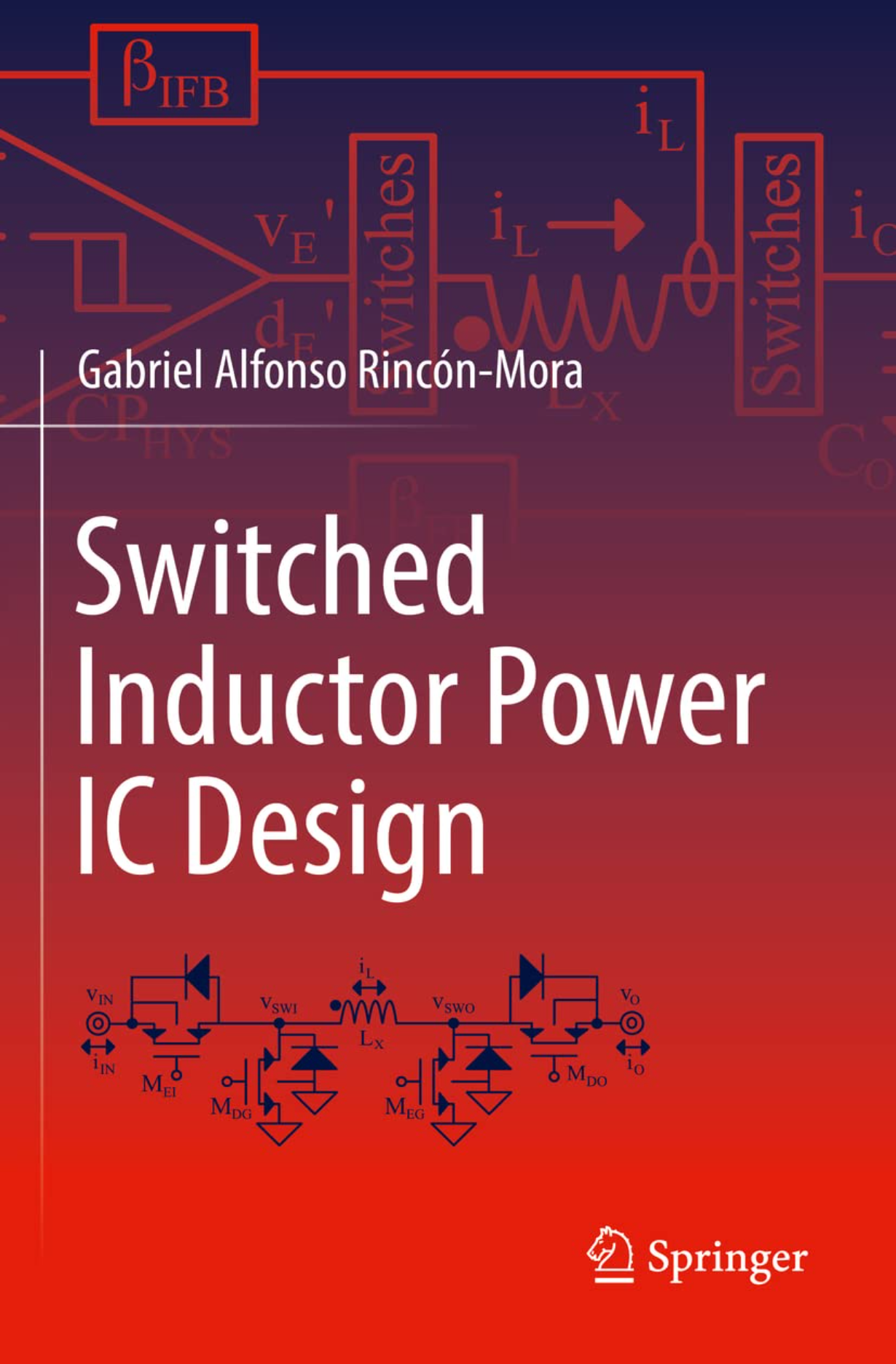
【教材】Switched Inductor Power IC Design
【教材】Switched Inductor Power IC Design
本教材通过设计见解、现实生活中的示例、图示、易于理解的方程以及简单的SPICE代码,展示了半导体器件(二极管、双极结型晶体管(BJT)和金属氧化物半导体(MOS)场效应晶体管(FET))在开关电感电源中如何独立和共同工作;这些电源如何传输功率、消耗功率以及在不同频率下的反应和响应;反馈回路如何对其进行切换、控制和稳定;以及构成这些电源的构建模块是如何实现和设计的。 本书内容重点突出且全面,以整体视角和方法探讨功率集成电路(IC)设计,涵盖从半导体器件到全闭环反馈系统的各个方面。读者将从中获得解读、评估和设计开关电感功率IC所需的洞察力,这些IC几乎是所有电子系统所必需的,而其他书籍则未以这种方式进行阐述。
完整版私信客服 186-6709-0885
![[Serdes]200Gbps高速串行接口发射机设计](https://material-image.wanwang.xin/1597234105050516/public/31e36bce-7552-450f-9726-ea5844ad6ca6.png)
[Serdes]200Gbps高速串行接口发射机设计
[Serdes]200Gbps高速串行接口发射机设计
本视频为英特尔高级设计团队工程师关于超高速串行通信接口(SerDes)发射机设计的学术报告。演讲者分享了其在英特尔十余年的高速电路设计经验,重点探讨了如何在先进FinFET CMOS工艺下实现200Gbps及以上数据率的线发射机设计。 报告内容涵盖: - 高速串行接口的技术背景与市场趋势,包括数据中心、AI芯片、光通信模块等应用场景 - 从25Gbps到224Gbps的技术演进路径及标准化进程 - PAM4调制技术、DAC+ADC架构、数字信号处理(DSP)等关键技术 - FinFET工艺下的设计挑战:带宽、噪声、线性度、可靠性权衡 - 时钟分布网络设计、抖动优化、相位校准技术 - 输出驱动器拓扑选择(电压模式/电流模式/混合模式) - 高速输出焊盘匹配网络与ESD设计 - 224Gbps发射机芯片实例:ISSCC 2023发表成果详解
完整版私信客服 186-6709-0885
CMOS比较器关键规格详解:偏移、迟滞、灵敏度与功耗仿真方法
CMOS比较器关键规格详解:偏移、迟滞、灵敏度与功耗仿真方法
视频标题 CMOS比较器关键规格详解:偏移、迟滞、灵敏度与功耗仿真方法 视频简介 本视频深入讲解CMOS比较器的核心性能指标及其测量方法。内容涵盖输入失调电压(系统性与随机性)、迟滞现象、电源灵敏度、灵敏度阈值、热噪声影响以及动态功耗等关键参数。通过Strong-Arm比较器实例,详细演示如何在仿真中测量这些指标,包括蒙特卡洛分析、瞬态噪声仿真等技术,帮助观众掌握比较器设计与验证的实用技能。 关键词 CMOS比较器, 输入失调电压, 迟滞, 电源抑制比, 比较器灵敏度, 热噪声, 动态功耗, 能量每比较, Strong-Arm锁存器, 蒙特卡洛仿真, 瞬态噪声分析, 亚稳态, 偏移校准, 再生比较器, 模拟IC设计
完整版私信客服 186-6709-0885
CMOS动态比较器原理与结构详解:从开环运放到高速锁存器设计-多伦多大学-Tony_Chan_Caruson
CMOS动态比较器原理与结构详解:从开环运放到高速锁存器设计-多伦多大学-Tony_Chan_Caruson
视频标题 CMOS动态比较器原理与结构详解:从开环运放到高速锁存器设计 --- 视频简介 本视频深入讲解CMOS比较器的结构与工作原理。首先分析为何不能直接采用开环运放作为比较器——补偿网络导致的低速主导极点会严重限制响应速度。随后介绍通过时钟控制断开米勒补偿电容来加速运放比较器的方法,并重点阐述现代CMOS技术中广泛应用的动态比较器(Dynamic Comparator)架构。 视频详细剖析动态比较器的核心工作机制:复位阶段(Reset)与再生阶段(Regeneration)的交替操作,以及正反馈回路如何实现指数级增长的差分电压放大。通过小信号模型推导,揭示再生时间常数与锁存速度的关键关系。同时介绍两种主流电路实现:StrongARM锁存器与双尾锁存器(Double-Tail Latch),对比它们在低电压应用中的优劣。 此外,视频还涵盖预放大器(Preamplifier)对抑制时钟反冲(Clock Kickback)的作用,以及RS锁存器后级如何消除输出波形的复位毛刺,最终得到干净的数字逻辑输出。适合模拟集成电路设计工程师及高年级电子专业学生系统学习高速比较器设计要点。 --- 关键词 CMOS比较器, 动态比较器, 开环运放, 米勒补偿, 正反馈锁存, StrongARM锁存器, 双尾锁存器, 再生时间常数, 时钟反冲, 预放大器, RS锁存器, 高速ADC, 模拟集成电路设计, 比较器速度优化, 低电压比较器
完整版私信客服 186-6709-0885
[比较器]27.CMOS动态比较器原理与结构详解:从开环运放到高速锁存器设计-多伦多大学Tony Chan Carusone
[比较器]27.CMOS动态比较器原理与结构详解:从开环运放到高速锁存器设计-多伦多大学Tony Chan Carusone
视频标题 CMOS动态比较器原理与结构详解:从开环运放到高速锁存器设计 --- 视频简介 本视频深入讲解CMOS比较器的结构与工作原理。首先分析为何不能直接采用开环运放作为比较器——补偿网络导致的低速主导极点会严重限制响应速度。随后介绍通过时钟控制断开米勒补偿电容来加速运放比较器的方法,并重点阐述现代CMOS技术中广泛应用的动态比较器(Dynamic Comparator)架构。 视频详细剖析动态比较器的核心工作机制:复位阶段(Reset)与再生阶段(Regeneration)的交替操作,以及正反馈回路如何实现指数级增长的差分电压放大。通过小信号模型推导,揭示再生时间常数与锁存速度的关键关系。同时介绍两种主流电路实现:StrongARM锁存器与双尾锁存器(Double-Tail Latch),对比它们在低电压应用中的优劣。 此外,视频还涵盖预放大器(Preamplifier)对抑制时钟反冲(Clock Kickback)的作用,以及RS锁存器后级如何消除输出波形的复位毛刺,最终得到干净的数字逻辑输出。适合模拟集成电路设计工程师及高年级电子专业学生系统学习高速比较器设计要点。 --- 关键词 CMOS比较器, 动态比较器, 开环运放, 米勒补偿, 正反馈锁存, StrongARM锁存器, 双尾锁存器, 再生时间常数, 时钟反冲, 预放大器, RS锁存器, 高速ADC, 模拟集成电路设计, 比较器速度优化, 低电压比较器
完整版私信客服 186-6709-0885
[比较器]28.CMOS比较器关键规格详解:偏移、迟滞、灵敏度与功耗仿真方法-多伦多大学Tony Chan Carusone
[比较器]28.CMOS比较器关键规格详解:偏移、迟滞、灵敏度与功耗仿真方法-多伦多大学Tony Chan Carusone
视频标题 CMOS比较器关键规格详解:偏移、迟滞、噪声与功耗测量方法 --- 视频简介 本视频深入讲解CMOS比较器的核心性能指标及其测量方法。内容涵盖:输入偏移电压(系统性与随机性来源)、迟滞现象的产生机理与测试、电源灵敏度分析、最小分辨灵敏度(metastability)、热噪声影响的量化方法,以及动态比较器的能量消耗评估。通过Strong-ARM比较器实例,详细演示蒙特卡洛仿真、瞬态噪声分析等实际测量技术,帮助观众掌握从电路设计到仿真验证的完整流程。 --- 关键词 CMOS比较器, 输入偏移电压, 迟滞, 电源抑制比, 比较器灵敏度, 亚稳态, 热噪声, 动态功耗, 能量/次比较, Strong-ARM锁存器, 蒙特卡洛仿真, 瞬态噪声分析, 随机失配, 系统性失配, 偏移校准, 再生比较器, 比较器测试方法
完整版私信客服 186-6709-0885
112Gbps 16nm CMOS TIA与共封装光电二极管:高灵敏度光接收器设计深度解析
112Gbps 16nm CMOS TIA与共封装光电二极管:高灵敏度光接收器设计深度解析
本视频来自多伦多大学的研究团队,详细展示了一款基于16nm CMOS工艺的112Gbps线性TIA(跨阻放大器)设计,并集成了共封装光电二极管,实现了-8.2dBm的高灵敏度。内容涵盖从系统架构到电路实现的全过程,包括PD(光电二极管)与接收器之间互连结构的优化、基于逆变器的TIA设计、以及采用PAM4调制的高速数据传输性能。视频中还展示了实际组装的共封装原型、电学与光学测量结果,并与现有先进研究进行了对比。该工作为400G/800G以太网光链路提供了高性能、低功耗的接收器解决方案,适合光通信、高速集成电路、封装集成等领域的研究人员与工程师参考。
完整版私信客服 186-6709-0885
【讲座】112Gbps 16nm CMOS TIA与共封装光电二极管:高灵敏度光接收器设计深度解析
【讲座】112Gbps 16nm CMOS TIA与共封装光电二极管:高灵敏度光接收器设计深度解析
本视频来自多伦多大学的研究团队,详细展示了一款基于16nm CMOS工艺的112Gbps线性TIA(跨阻放大器)设计,并集成了共封装光电二极管,实现了-8.2dBm的高灵敏度。内容涵盖从系统架构到电路实现的全过程,包括PD(光电二极管)与接收器之间互连结构的优化、基于逆变器的TIA设计、以及采用PAM4调制的高速数据传输性能。视频中还展示了实际组装的共封装原型、电学与光学测量结果,并与现有先进研究进行了对比。该工作为400G/800G以太网光链路提供了高性能、低功耗的接收器解决方案,适合光通信、高速集成电路、封装集成等领域的研究人员与工程师参考。
完整版私信客服 186-6709-0885
【讲座】迈向低功耗和专用无线通信-Patrick Mercier
【讲座】迈向低功耗和专用无线通信-Patrick Mercier
无
完整版私信客服 186-6709-0885
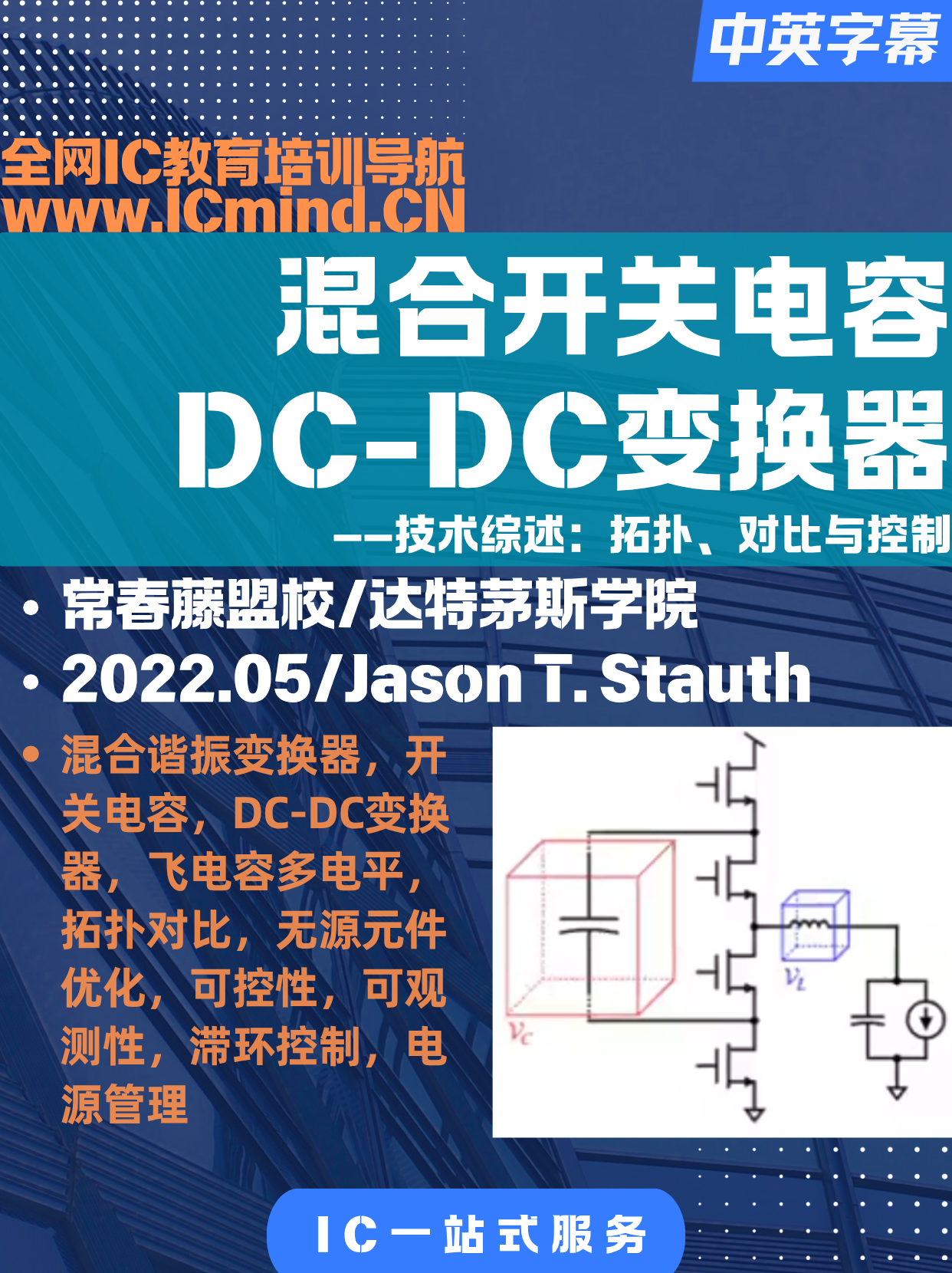
混合开关电容DCDC技术综述2022
混合开关电容DCDC技术综述2022
达特茅斯学院Jason Stealth教授系统介绍了混合谐振开关电容变换器的研究进展,涵盖拓扑分类、性能对比、无源元件优化、可控性与可观测性分析,以及非线性控制技术,展示了该领域十余年的研究成果与未来发展方向。 大纲: 1. 开场与背景介绍 2. 电源管理的重要性:移动设备、高性能计算、可再生能源、汽车电子等应用场景 3. DC-DC变换器的基本抽象:开关过程、能量存储、整流过程及损耗维度 4. 无源元件特性对比:电容与电感的能量密度差异(电容优势显著) 5. 混合谐振开关电容变换器的核心理念:利用高能量密度电容完成大部分电压转换,减小电感体积 6. 拓扑发展历史:从1988年Middlebrook的论文到现代应用 7. 基础开关电容拓扑类别: - 串并联架构(最佳电容利用率) - Dixon梯/科克罗夫特-沃尔顿架构(最佳有源器件利用率) - 飞电容多电平变换器(多输出、频率倍增) - 倍压器型拓扑(最高变比) 8. 拓扑性能对比:基于最小功率损耗品质因数,考虑开关频率与无源元件体积约束 9. 电感损耗与尺寸优化:电感与电容体积存在最优分配比例(1/4至3/5) 10. 拓扑选择取决于应用:开关电压应力缩放模型影响最优拓扑选择 11. 控制挑战:飞电容电压不平衡问题,高阶系统的可控性与可观测性分析 12. 非线性控制方法:滞环/滑模控制实现快速平衡与软启动 13. ISSCC 2021实现案例:25微秒恢复时间、10微秒启动 14. 未来展望:控制概念、平衡启动、电平移位策略、低成本实现、自举电容设计
完整版私信客服 186-6709-0885
【教材】Operational Amplifier
【教材】Operational Amplifier
本书涵盖运算放大器的多个方面,包括理论解释以及简化的表达式和推导。本书旨在作为电子与通信工程专业本科生和研究生课程的教材。内容包括直流放大器、直流放大器的交/直流分析、相关推导、运算放大器的框图、正反馈与负反馈、调幅器、电流-电压和电压-电流转换器、数模转换器(DAC)和模数转换器(ADC)、积分器、微分器、有源滤波器、比较器、正弦和非正弦波形发生器、锁相环(PLL)等。本书分为A和B两部分。A部分包括理论、方法、电路设计和推导。B部分解释实验室实践的实验设计和研究。实验室实验使学生能够进行实际操作,展示运算放大器的应用。对电路、工作原理的简化描述以及理解概念的实用方法是本书的独特之处。对于没有任何电子学背景知识的读者,本书的其他特点包括推导方法简单、步骤易懂以及表述清晰。本书以学生为中心,围绕运算放大器的基础知识及其应用展开。详细的内容覆盖和教学工具使其成为电子与通信工程专业高年级本科生和低年级研究生课程的理想教材。
完整版私信客服 186-6709-0885
【教材】Analog Circuits for Machine Learning
【教材】Analog Circuits for Machine Learning
由工业界和学术界专家撰写,提供模拟电路设计领域的最新参考资料 以教程形式呈现内容 涵盖高性能模数和数模转换器、物联网智能传感器以及亚1V和先进节点模拟电路设计
完整版私信客服 186-6709-0885
IEEE-研讨会-印度-03-MATLAB 辅助混合信号 IC 优化设计:从晶体管级仿真到系统级性能提升
IEEE-研讨会-印度-03-MATLAB 辅助混合信号 IC 优化设计:从晶体管级仿真到系统级性能提升
本视频为2022年IEEE SSCS工程系统建模与仿真研讨会的第二部分进阶课程,由MathWorks专家系统讲解如何利用MATLAB/Simulink实现从算法到芯片的高效设计闭环。课程对比了MATLAB代码建模与Simulink框图建模的差异,重点展示Simulink内置时间引擎优势,以数字滤波器为案例演示全流程,剖析Sigma-Delta ADC高层级行为建模及协同仿真,介绍“左移验证”理念及Simscape物理建模库应用,为相关工程师与研究人员提供标准化建模方法论。
完整版私信客服 186-6709-0885
[SerDes]200Gbps高速串行接口发射机设计:CMOS技术实现与挑战
[SerDes]200Gbps高速串行接口发射机设计:CMOS技术实现与挑战
视频标题: 200Gbps高速串行接口发射机设计:CMOS技术实现与挑战 视频简介: 本视频为英特尔高级设计团队工程师关于超高速串行通信接口(SerDes)发射机设计的学术报告。演讲者分享了其在英特尔十余年的高速电路设计经验,重点探讨了如何在先进FinFET CMOS工艺下实现200Gbps及以上数据率的线发射机设计。 报告内容涵盖: - 高速串行接口的技术背景与市场趋势,包括数据中心、AI芯片、光通信模块等应用场景 - 从25Gbps到224Gbps的技术演进路径及标准化进程 - PAM4调制技术、DAC+ADC架构、数字信号处理(DSP)等关键技术 - FinFET工艺下的设计挑战:带宽、噪声、线性度、可靠性权衡 - 时钟分布网络设计、抖动优化、相位校准技术 - 输出驱动器拓扑选择(电压模式/电流模式/混合模式) - 高速输出焊盘匹配网络与ESD设计 - 224Gbps发射机芯片实例:ISSCC 2023发表成果详解 本报告适合集成电路设计、高速通信系统、混合信号电路等领域的研究人员和工程师参考。 关键词: 高速串行接口,SerDes,发射机设计,200Gbps,PAM4调制,CMOS集成电路,FinFET工艺,时钟抖动,数模转换器,DAC,数字信号处理,DSP,高速IO设计,光通信,以太网,信号完整性,线性度优化,抖动均衡,集成电路设计,ISSCC
完整版私信客服 186-6709-0885
IEEE-研讨会-圣地亚哥分会-三星-5G毫米波终端收发器设计深度解析:架构创新与电路挑战
IEEE-研讨会-圣地亚哥分会-三星-5G毫米波终端收发器设计深度解析:架构创新与电路挑战
视频标题 5G毫米波终端收发器设计深度解析:架构创新与电路挑战 --- 视频简介 本次讲座由三星高级电路设计组的Vino Baga主讲,深入探讨5G毫米波(FR2频段)移动终端(UE)收发器设计的核心挑战与创新方向。内容涵盖: - 5G毫米波背景:为何选择毫米波频段、相控阵技术原理及其在移动终端的特殊约束 - 系统架构对比:RF接口、IF接口、基带分布式等四种主流架构的权衡分析 - 发射机关键挑战:CMOS功率放大器设计、堆叠PA架构、T/R开关损耗优化、功率控制与校准 - 接收机创新方向:宽带LNA设计、多频段合并、载波聚合实现 - 时钟与相位噪声:高频下PLL设计的独特约束 - 系统级考量:模组尺寸、电池寿命、散热管理与产品形态的平衡 讲座结合产业界最新研究成果(IBM、Broadcom、UCSD等),为射频/模拟IC设计工程师、无线通信研究人员及5G技术从业者提供前沿技术洞察。 --- 关键词 5G毫米波、毫米波收发器、相控阵、功率放大器、CMOS射频IC、FR2频段、终端设计、T/R开关、相位噪声、堆叠PA、宽带LNA、载波聚合、射频架构、三星、IEEE SSCS
完整版私信客服 186-6709-0885

SRAM存内计算:面向高能效AI系统的芯片设计前沿
SRAM存内计算:面向高能效AI系统的芯片设计前沿
本视频为2021年首尔国立大学E-Tech Talks夏季讲座,主讲人详细介绍了基于SRAM的存内计算(In-Memory Computing, IMC)技术及其在AI加速器中的应用。内容涵盖:AI芯片面临的数据移动瓶颈问题、存内计算的基本原理与优势、不同存储技术(SRAM/DRAM/RRAM/PCM)的对比分析、模拟存内计算的电路实现方案(阻性/容性)、ADC设计优化策略,以及团队最新研究成果——集成108个宏单元的可编程存内计算加速器PIMCA。此外还介绍了IMC噪声建模、噪声感知训练算法,以及利用硬件噪声提升对抗鲁棒性的创新思路。适合对AI芯片、存内计算、边缘计算感兴趣的科研人员与工程师观看。
完整版私信客服 186-6709-0885
IEEE-研讨会-圣地亚哥分会-Chiplet架构与未来计算技术-AMD高级副总裁Sam Naffziger深度解析
IEEE-研讨会-圣地亚哥分会-Chiplet架构与未来计算技术-AMD高级副总裁Sam Naffziger深度解析
本视频为IEEE圣地亚哥/柯林斯堡分会2021年7月网络研讨会内容,特邀AMD高级副总裁兼企业院士Sam Naffziger(拥有超30年半导体行业经验,主导多项低功耗技术与Chiplet架构创新)发表主题演讲,探讨了全球计算需求增长与摩尔定律放缓的矛盾、机器学习训练算力需求挑战、专用加速器与模块化设计趋势、AMD Chiplet架构演进、硅片封装协同设计突破及相关封装技术权衡分析,适合芯片架构师等半导体行业从业者观看。
完整版私信客服 186-6709-0885

仪表放大器原理与改进设计详解 多伦多大学 Tony_Chan_Carusone
仪表放大器原理与改进设计详解 多伦多大学 Tony_Chan_Carusone
视频标题 仪表放大器原理与改进设计详解 | 从基础差分放大到三运放仪表放大器 --- 视频简介 本视频深入讲解仪表放大器(Instrumentation Amplifier)的工作原理与设计改进。首先介绍基础差分放大器的局限性——有限的输入阻抗和共模信号处理问题;随后分析通过添加非反相缓冲级获得高输入阻抗的初步方案,并指出其共模信号被第一级放大的隐患;最后详细剖析经典的三运放仪表放大器结构,解释去掉接地电阻后如何实现第一级共模抑制,从而避免运放饱和和信号失真。适合学习模拟电路设计、传感器信号调理和精密测量的工程师与学生。 --- 关键词 仪表放大器、差分放大器、共模抑制比、高输入阻抗、三运放结构、运算放大器、传感器信号调理、精密测量、虚拟短路、非反相放大器、生物医学信号、应变片测量、模拟电路设计
完整版私信客服 186-6709-0885
[英飞凌×微软]800G光模块技术竞赛:数据中心下一代互联技术解析
[英飞凌×微软]800G光模块技术竞赛:数据中心下一代互联技术解析
视频标题 800G光模块技术竞赛:数据中心下一代互联技术解析 --- 视频简介 本视频深入探讨800G光模块技术的最新发展趋势,特邀Infinera技术专家Radha Nagarajan与Ilya Lyubomirsky,以及微软云网络架构师Mark Filer共同参与。 内容亮点: - 技术演进路径:从400G到800G的技术跨越,解析200G/lambda PAM4调制技术的关键优势 - 数据中心架构变革:扁平化网络架构趋势,以及交换机端口密度(Radix)如何驱动互联速率升级 - 工程权衡分析:深入对比PAM4、PAM6等调制格式的SNR要求、功耗与实现复杂度 - 微软视角: hyperscale云运营商对800G部署的现实考量,包括功耗瓶颈、CPO(共封装光学)技术路线,以及网络架构优化策略 - FEC与DSP创新:低功耗前向纠错编码与均衡技术的最新进展 无论您是光通信工程师、数据中心架构师,还是关注下一代网络基础设施的技术决策者,本视频都将为您提供800G技术发展的全面洞察。 --- 关键词 800G光模块、数据中心互联、PAM4调制、硅光技术、共封装光学(CPO)、DSP数字信号处理、前向纠错(FEC)、交换机架构、光通信、超大规模数据中心、400G ZR、200G/lambda、网络功耗优化、TOR架构、微软Azure
完整版私信客服 186-6709-0885
IEEE-研讨会-圣地亚哥分会-Micron GDDR6X技术深度解析:全球首款单端PAM4显存接口如何实现22Gbps带宽突破
IEEE-研讨会-圣地亚哥分会-Micron GDDR6X技术深度解析:全球首款单端PAM4显存接口如何实现22Gbps带宽突破
本视频为Micron院士Tim Hollis博士的技术演讲,详细介绍GDDR6X显存架构的创新设计。作为ISSCC 2020备受好评论文的返场演讲,Hollis博士分享了如何通过单端PAM4信号编码技术,在标准DRAM工艺中实现22Gbps/pin的带宽突破,同时将核心频率从9GHz降至5.5GHz,显著提升能效比。 演讲涵盖:GDDR显存技术演进历程、PAM4接口架构设计、发送端/接收端电路拓扑、封装信号完整性优化、实测性能数据,以及未来技术发展方向。适合存储器设计工程师、高速接口设计人员及半导体行业从业者观看。
完整版私信客服 186-6709-0885
IEEE-研讨会-圣地亚哥分会-Micron GDDR6X技术深度解析:全球首款单端PAM4显存接口如何实现22Gbps带宽突破
IEEE-研讨会-圣地亚哥分会-Micron GDDR6X技术深度解析:全球首款单端PAM4显存接口如何实现22Gbps带宽突破
本视频为Micron院士Tim Hollis博士的技术演讲,详细介绍GDDR6X显存架构的创新设计。作为ISSCC 2020备受好评论文的返场演讲,Hollis博士分享了如何通过单端PAM4信号编码技术,在标准DRAM工艺中实现22Gbps/pin的带宽突破,同时将核心频率从9GHz降至5.5GHz,显著提升能效比。 演讲涵盖:GDDR显存技术演进历程、PAM4接口架构设计、发送端/接收端电路拓扑、封装信号完整性优化、实测性能数据,以及未来技术发展方向。适合存储器设计工程师、高速接口设计人员及半导体行业从业者观看。
完整版私信客服 186-6709-0885
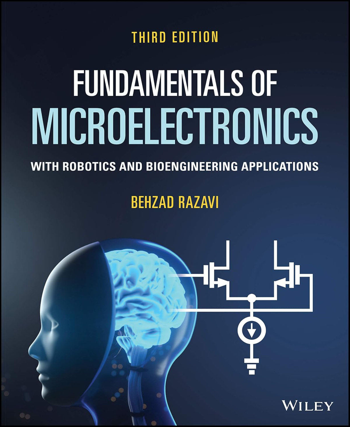
【教材】Fundamentals of Microelectronics 3rd Edition
【教材】Fundamentals of Microelectronics 3rd Edition
《微电子学基础》(第三版)是一本全面介绍电路设计与分析的书籍,旨在帮助学生培养在未来职业生涯中取得成功所必需的实践技能和工程直觉。通过创新的“通过检查进行分析”框架,学生学会将复杂问题分解为熟悉的组件,并利用基本原理找到解决方案。微电子学的循序渐进综合方法展示了每个器件在电路中的作用,同时帮助学生树立“以设计为导向”的思维方式。 第三版修订版涵盖了基本的半导体物理学、二极管模型和电路、双极型晶体管和放大器、振荡器、频率响应等内容。深入章节配有说明性示例和大量难度各异的问题,包括设计问题,挑战学生选择偏置和元件值以满足特定要求。本书包含丰富的教学工具,如应用侧栏、章节总结、带答案的自测题以及Multisim和SPICE软件仿真问题。现推出增强版ePub格式,《微电子学基础》是该学科单学期和双学期课程的理想选择。
完整版私信客服 186-6709-0885
【教材】Semiconductor Advanced Packaging
【教材】Semiconductor Advanced Packaging
本书重点介绍先进半导体封装组件和系统的设计、材料、工艺、制造及可靠性。书中既阐述了原理,也涉及工程实践,且更侧重于工程实践。这通过深入研究多个主要主题来实现,例如系统级封装、扇入型晶圆/面板级芯片级封装、扇出型晶圆/面板级封装、2D、2.1D、2.3D、2.5D和3D集成电路集成、芯粒封装、芯片到晶圆键合、晶圆到晶圆键合、混合键合以及用于高速高频的介电材料。本书可为电气工程、机械工程、材料科学和工业工程等领域的研究人员、工程师和研究生提供帮助。
完整版私信客服 186-6709-0885
【课程】通往200Gbps串行链路的路径:技术挑战与未来展望
【课程】通往200Gbps串行链路的路径:技术挑战与未来展望
在本视频中,资深高速串行接口专家深入探讨了实现200Gbps串行链路所面临的技术挑战与解决方案。内容涵盖从112Gbps迈向200Gbps的关键技术演进,包括不同调制方案(如PAM4、PAM8、QAM)的优劣比较、信道损耗的影响、以及如何通过前向纠错(FEC)和DSP架构提升信号完整性。演讲还对比了模拟与数字信号处理(DSP)架构的性能差异,并展望了未来电气信号与硅光子学在超高速互联中的角色。适合半导体、通信、数据中心等相关领域的工程师、架构师和技术决策者观看。
完整版私信客服 186-6709-0885
【教材】TRANSFE FUNCTIONS OF SWITCHING CONVERTERS
【教材】TRANSFE FUNCTIONS OF SWITCHING CONVERTERS
《开关变换器的传递函数》教授读者如何确定消费和工业市场中常见的开关电源的传递函数。本书从开关单元的平稳介绍开始,深入讲解线性化和小信号调制的第一步细节。然后,您将学习PWM开关模型的推导过程,以及如何将其应用于以固定开关频率运行的基本结构,以及电压或电流模式控制下的各种工作条件,如连续和不连续模式。该模型被扩展到其他控制方案,如准谐振、恒定导通时间和关断时间转换器,所有这些都有相关的小信号版本。接下来的章节探讨了基本结构,如降压、升压和升降压单元,之后涵盖了它们的隔离版本,如正激或反激转换器。最后一章讨论更复杂的结构,如Cuk、Zeta、SEPIC和LLC。
完整版私信客服 186-6709-0885
IEEE-研讨会-圣地亚哥分会-亚16纳米工艺下千兆采样率ADC的设计挑战与产学研协作路径
IEEE-研讨会-圣地亚哥分会-亚16纳米工艺下千兆采样率ADC的设计挑战与产学研协作路径
视频标题 《亚16纳米工艺下千兆采样率ADC的设计挑战与产学研协作路径》——Doug Smith技术演讲 --- 视频简介 本视频为NXP资深技术专家Doug Garrity关于高速模数转换器(ADC)设计的专题技术演讲。演讲以数字调制雷达(DMR)为典型应用场景,深入分析了在16纳米及以下先进工艺节点实现千兆采样率(GS/s)ADC所面临的架构选择、功耗优化、时钟抖动、时间交织等核心技术挑战。 Smith先生通过大量IEEE会议论文数据对比,揭示了学术界与工业界在ADC研究成果上的显著差异:学术界专注于Walden优值(FOM)的极致优化,而工业界更关注实际应用中的可靠性、温度范围、抗干扰性和量产良率。他重点展示了IBM 72GS/s 8位ADC、日本鹿儿岛大学时间域ADC以及NXP混合架构ADC等三个典型案例,论证了时间域量化、VCO-based架构等创新方向在先进工艺下的发展潜力。 演讲最后发出行动呼吁,强调必须通过产学研深度合作、政府与代工厂协同支持,解决高校研究者获取亚16纳米工艺资源的难题,才能推动高速ADC技术的实质性突破。内容对射频收发芯片、5G通信、汽车雷达等领域的工程师和研究人员具有重要参考价值。 --- 关键词 `模数转换器、ADC、千兆采样率、GS/s ADC、16纳米工艺、FinFET、时间交织、数字调制雷达、DMR雷达、FMCW、Walden优值、FOM、时间域量化、VCO-based ADC、流水线ADC、时钟抖动、时钟偏斜、IBM 72GS/s ADC、汽车雷达、5G通信、射频收发器、SoC集成、产学研合作、工艺资源获取、TSMC、三星代工、SkyWater、IEEE ISSCC、CICC、SRC、NSF`
完整版私信客服 186-6709-0885
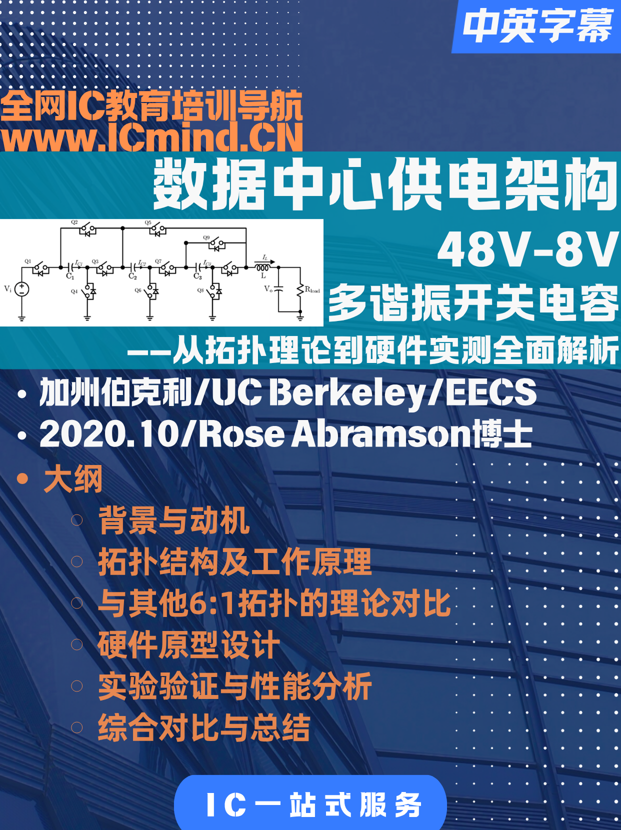
2020_UC伯克利_数据中心供电架构48V转8V
2020_UC伯克利_数据中心供电架构48V转8V
随着AI计算和云服务的爆发式增长,数据中心耗电量已占全球电力消耗的1%,供电效率成为行业核心挑战。近年来,业界从传统12V母线转向48V配电架构以减少传导损耗,但如何将48V高效、高密度地降至负载所需电压(如8V)仍是设计难点。 本期演讲来自加州大学伯克利分校博士候选人Rose,她介绍了一款专为48V至8V降压设计的六比一多谐振级联串并联开关电容转换器。该拓扑采用三阶段谐振工作模式(两相串联、一相并联),仅需10个功率开关和3个飞电容,且仅使用单个输出电感,元件数量显著少于同类六比一谐振方案。 硬件原型在48V输入、40A满载条件下,功率级峰值效率达99%,含栅极驱动损耗后仍达98.5%,满载效率为97.1%,功率密度高达2230瓦每立方英寸。通过准谐振控制实现准零电流开关,所有开关均采用标准硅基MOSFET,无需氮化镓器件,兼顾成本与可靠性。 视频详细讲解了拓扑工作原理、设计约束、与Dickson、串并联、飞电容多电平、开关谐振腔等主流拓扑的理论对比,并展示了PCB布局、栅极驱动、热管理、效率曲线、负载动态响应等完整实验验证过程。适合电力电子工程师、数据中心硬件设计师及电源领域研究人员观看。 关键词:高转换比开关电容,多谐振变换器,48V转8V,数据中心供电,高效率99%,功率密度,串并联拓扑,零电流开关,中间母线电压,硅基MOSFET
完整版私信客服 186-6709-0885
![[TI]CDR技术全解析:高速信号传输的“隐形守护者”](https://material-image.wanwang.xin/1597234105050516/public/c9275436-e55f-4a0d-b1dc-2cb961998a14.png)
[TI]CDR技术全解析:高速信号传输的“隐形守护者”
[TI]CDR技术全解析:高速信号传输的“隐形守护者”
引言:CDR在高速通信中的角色 CDR核心功能:从数据中恢复时钟 CDR的关键技术参数详解 锁相环(PLL)架构 抖动传输(Jitter Transfer) 抖动生成(Jitter Generation) 抖动容限(Jitter Tolerance) 实战考量:如何选择最佳CDR? 总结与展望
完整版私信客服 186-6709-0885
IEEE-研讨会-圣地亚哥分会-PCI Express 6.0技术深度解析:64GT/s PAM4信号下的低延迟高带宽互连方案
IEEE-研讨会-圣地亚哥分会-PCI Express 6.0技术深度解析:64GT/s PAM4信号下的低延迟高带宽互连方案
本视频为Intel院士Devendra Das Sharma博士在IEEE圣地亚哥联合分会举办的网络研讨会上的技术演讲。作为PCIe和CXL标准的关键推动者,Sharma博士系统介绍了PCI Express 6.0规范的核心技术创新,包括PAM4信号技术、FLIT模式架构、延迟优化策略、可靠性设计及向后兼容性。演讲还涵盖了PCIe在数据中心、云计算、边缘计算及汽车电子等领域的应用趋势,以及与CXL标准的协同关系,适合高速接口设计工程师、系统架构师及计算机体系结构研究人员观看。
完整版私信客服 186-6709-0885
IEEE-研讨会-圣地亚哥分会-IBM专家深度解析:56-128Gbps高速串行发射器设计与PAM4调制技术
IEEE-研讨会-圣地亚哥分会-IBM专家深度解析:56-128Gbps高速串行发射器设计与PAM4调制技术
本视频为IEEE固态电路学会(SSCS)特邀讲座,由IBM T.J. Watson研究中心的Todd Dixon博士主讲。Dixon博士是SSCS杰出讲师,曾获得多项最佳论文奖项。 讲座核心内容: 📡 高速通信背景:数据中心网络对高带宽互连的需求,从28G NRZ到56G/112G/224G PAM4的技术演进 🔧 发射器架构设计: - 传统模拟混合信号方案 vs. DAC/ADC数字方案 - 前馈均衡器(FFE)与驱动器拓扑(CML电流模 vs. SST电压模) ⚡ 两个设计实例深度剖析: 1. 56Gbps PAM4发射器:采用T/2半波特间隔均衡器的创新时钟相位选择技术 2. 128Gbps PAM4发射器:高分辨率温度计编码CML驱动器,实现200μV精细抽头控制 🔮 未来展望:200Gbps及以上速率的挑战,多音传输(DMT)与光电共封装(CPO)技术趋势
完整版私信客服 186-6709-0885
IEEE-研讨会-圣地亚哥分会-从5G到6G的半导体技术挑战与未来趋势-高通副总裁
IEEE-研讨会-圣地亚哥分会-从5G到6G的半导体技术挑战与未来趋势-高通副总裁
本视频为IEEE圣地亚哥分会2021年10月网络研讨会录像,特邀高通公司工艺技术与代工工程副总裁Chidi Chidambaram博士(IEEE会士、应变工程与SOI晶体管开发领域先驱者)发表主题演讲,探讨半导体行业关键技术挑战及5G向6G演进所需的创新突破,内容涵盖5G/6G愿景与应用场景、技术范式转变、射频前端集成挑战、芯片技术路线、关键器件演进、异构集成与系统级协同优化等,并设有问答环节讨论光子集成、量子计算应用及5G物联网成本等热点。
完整版私信客服 186-6709-0885
【DCDC】电压模式 vs 电流模式控制:40年实战专家深度解析
【DCDC】电压模式 vs 电流模式控制:40年实战专家深度解析
大纲 1. 开场与准备 - webinar背景、软件下载说明、参会者互动 2. 电压模式控制详解 - 降压变换器规格设定(48V→12V@10A) - LC滤波器特性、环路补偿设计(Type 3补偿器) - 关键指标:环路增益、输出阻抗、音频抑制比(PSRR) - 仿真演示:轻载断续模式(DCM)下的性能退化问题 3. 电流模式控制剖析 - 基本原理:同时检测电压与电流(开关电流或电感电流) - 功率级特性:单极点 vs 实际三极点(半开关频率处的双极点) - 斜坡补偿对Q值的影响 - 多路并联均流优势 4. 电压模式 vs 电流模式全面对比 - 小信号响应:环路增益族曲线(电流模式在DCM下仍稳定) - 大信号阶跃负载:电流模式过冲更小、阻尼更好 - 音频抑制比:电流模式明显优于电压模式 - 输出阻抗:两者低频相近,中频段电流模式更优 5. 工程实践与前沿挑战 - 高频、高集成度下电流传感的难题(无空间放电流互感器或电阻) - 解决方案:无损耗电感辅助绕组传感 + 观测器/状态估计器 - 电压模式前馈(feed-forward)仅为“半成品”电流模式 - 数字控制的局限与建议 6. 工具与资源 - Ridley Works软件演示(实时调整参数、多环路扫描) - Ridley Box(频率响应分析仪+示波器+嵌入式电脑) - 免费书籍、论文、Facebook设计社区、后续webinar预告 7. 问答与总结 - 相位裕度45°的意义、输出阻抗平坦化误区、多相均流等热点问题解答 - 倡导“先模拟后数字”的设计流程
完整版私信客服 186-6709-0885
![[TI]RF PLL 关键参数详解-频率综合器/相位噪声/锁相环](https://material-image.wanwang.xin/1597234105050516/public/e00b9fb7-f5db-47ca-8409-81b71847196b.png)
[TI]RF PLL 关键参数详解-频率综合器/相位噪声/锁相环
[TI]RF PLL 关键参数详解-频率综合器/相位噪声/锁相环
简介 本视频系统讲解RF锁相环(PLL)和频率合成器中的核心参数与规格,包括鉴相频率、电荷泵电流、VCO增益、相位噪声、杂散及锁定时间等。内容涵盖各参数的定义、对系统性能的影响,以及在实际设计(尤其是环路滤波器设计)中的应用。同时介绍了TI的在线/离线设计工具(Clock Architect、PLLATINUMSIM)如何辅助选型和仿真。最后通过典型问答澄清常见误区,帮助工程师实现干净、稳定的PLL设计。
完整版私信客服 186-6709-0885
[LDO]ISSCC2020-edu-数字低压差集成稳压器(Digital LDO)基础教程
[LDO]ISSCC2020-edu-数字低压差集成稳压器(Digital LDO)基础教程
本教程由哥伦比亚大学副教授Mingo主讲,聚焦数字低压差集成稳压器(Digital LDO)的核心知识。内容涵盖数字LDO的基本架构、与模拟LDO的对比、关键性能指标、主流技术分类及稳定性分析方法,并提及相关资源获取途径与固态电路协会(SSCS)会员福利。
完整版私信客服 186-6709-0885
边缘计算芯片架构革新:Quadric如何用统一架构破解低延迟与高能效难题
边缘计算芯片架构革新:Quadric如何用统一架构破解低延迟与高能效难题
半导体工程主编Ed Sperling专访Quadric联合创始人Nigel Drago,深入探讨边缘计算芯片架构的演进趋势。传统云端处理器架构因功耗过高、延迟过大难以适应边缘场景,Quadric提出"通用NPU"创新方案——通过将CPU与NPU紧密集成于单一架构,配合近内存计算设计,大幅减少数据搬运带来的能耗与延迟。Nigel详细解析了边缘AI处理的核心挑战:从异构计算的软件分区难题,到AI算法快速迭代对硬件灵活性的要求,以及Quadric如何通过软硬件协同设计实现"一次流片、持续适配"的目标。本访谈为理解自动驾驶、机器人等实时边缘应用的芯片设计提供了关键洞察。
完整版私信客服 186-6709-0885
【讲座】高性能ADC中的运算放大器的设计
【讲座】高性能ADC中的运算放大器的设计
无
完整版私信客服 186-6709-0885
【讲座】ADC性能极限
【讲座】ADC性能极限
无
完整版私信客服 186-6709-0885
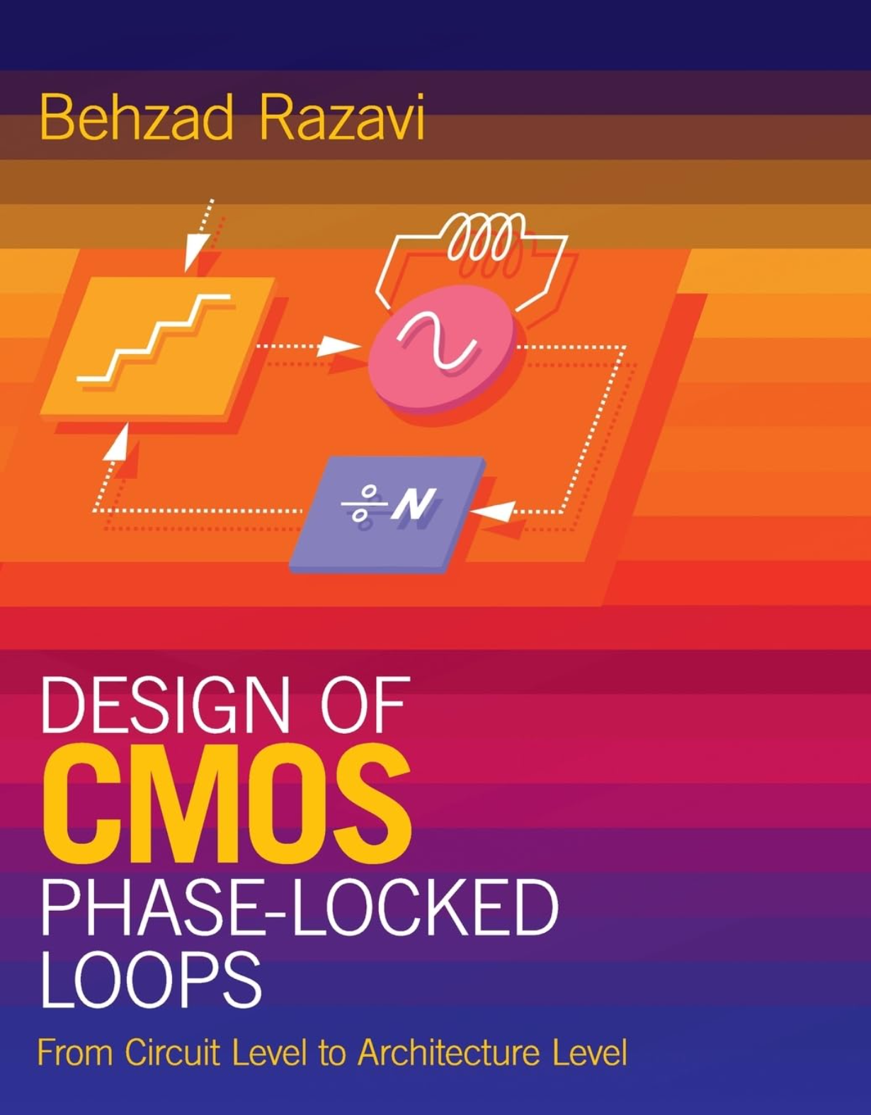
【教材】Design of CMOS Phase-Locked Loops: From Circuit Level to Architecture Level
【教材】Design of CMOS Phase-Locked Loops: From Circuit Level to Architecture Level
本教材采用现代教学法,为学生和工程师提供了关于CMOS锁相环(PLL)设计的全面而严谨的知识,适用于广泛的应用场景。它以直观的方式呈现理论概念,从最简单的形式逐步构建到更实用的系统;广泛涵盖关键主题,包括振荡器、相位噪声、模拟PLL、数字PLL、射频合成器、延迟锁定环、时钟和数据恢复电路以及分频器;包含关于高性能振荡器设计的教程章节,涵盖从基础到高级拓扑结构的内容;并大量使用电路仿真来教授设计思维,突出设计缺陷,并将理论与实践相结合。本书包含200多个发人深省的示例,重点介绍最佳实践和常见陷阱;250个章节末的课后作业问题,用于测试和增强读者的理解;以及为教师提供的解决方案和讲座幻灯片,是希望深入了解PLL设计的高级本科生、研究生和专业工程师的完美教材。
完整版私信客服 186-6709-0885
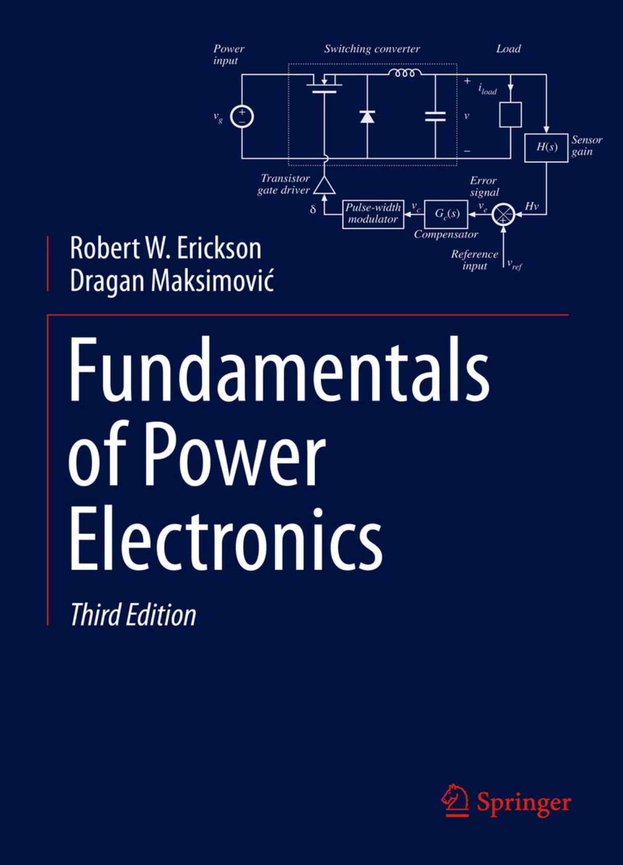
【教材】Fundamentals of Power Electronics Third Edition
【教材】Fundamentals of Power Electronics Third Edition
《电力电子基础》(第三版)是一本关于电力电子领域的最新且权威的教科书和参考书。新版保留了原版的初衷和理念,即专注于设计实用电力电子系统所需的基本原理、模型和技术要求,同时增添了大量新材料。新版的主要改进包括:增加了关于开关损耗机制及其建模的新内容;引入了宽禁带半导体器件;对平均方法进行了更严谨的处理;阐述了奈奎斯特稳定性判据;纳入了用于电流程序控制的Tan和Middlebrook模型;新增了一章关于开关变换器的数字控制;新增了多章关于设计导向分析的高级技术,包括反馈和额外元件定理、平均电流控制;增加了关于输入滤波器设计的新内容;对平均开关建模、仿真和间接功率进行了新的处理;以及探讨了DCM、CPM和数字控制中的采样效应。
完整版私信客服 186-6709-0885
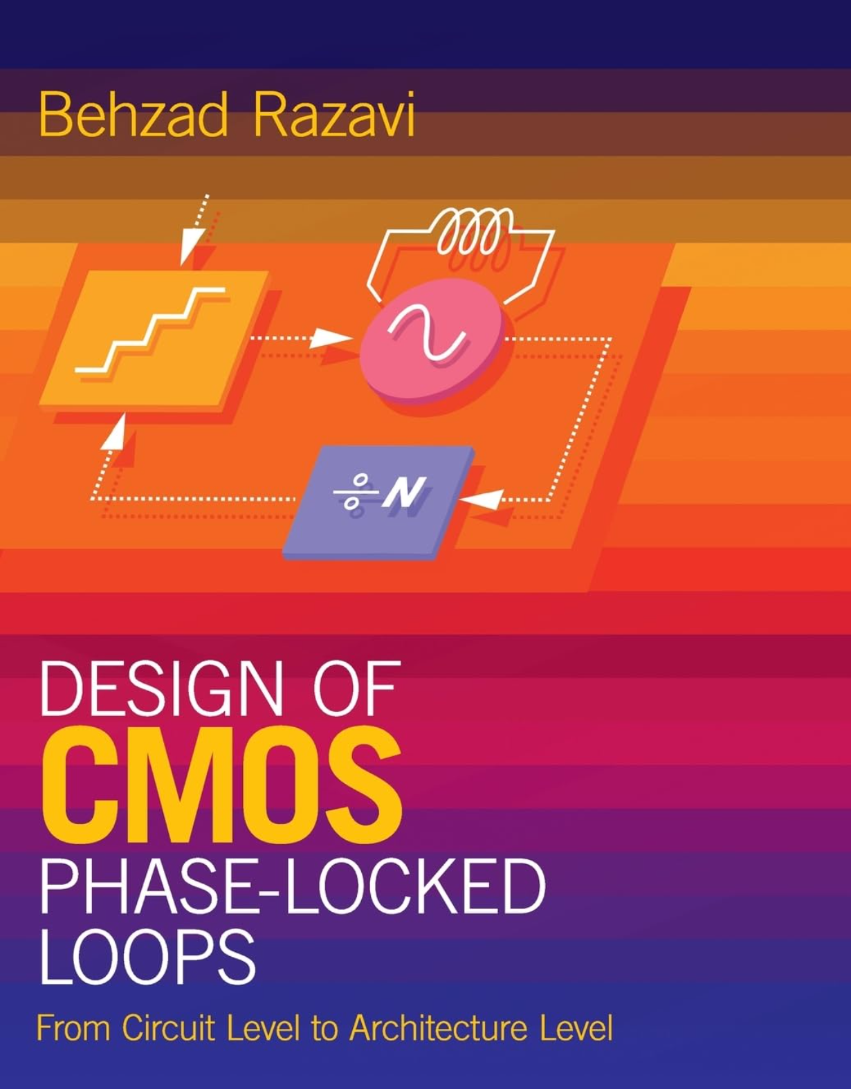
【教材】Design of CMOS Phase-Locked Loops: From Circuit Level to Architecture Level
【教材】Design of CMOS Phase-Locked Loops: From Circuit Level to Architecture Level
本书采用现代教学法,为学生和工程师提供了关于CMOS锁相环(PLL)设计的全面而严谨的知识,适用于广泛的应用场景。本书以直观的方式呈现理论概念,从最简单的形式逐步构建到更实用的系统;广泛涵盖关键主题,包括振荡器、相位噪声、模拟PLL、数字PLL、射频合成器、延迟锁定环、时钟和数据恢复电路以及分频器;设有关于高性能振荡器设计的教程章节,涵盖从基础到高级拓扑结构的内容;大量使用电路仿真来教授设计思维,突出设计缺陷,并将理论与实践相结合。本书包含200多个发人深省的示例,突出最佳实践和常见陷阱,250个章节末的课后作业问题以测试和增强读者的理解,以及为教师提供的解决方案和讲座幻灯片,是希望深入了解PLL设计的高级本科生、研究生和专业工程师的完美教材。
完整版私信客服 186-6709-0885
【教材】Fundamentals of Layout Design for Electronic Circuits
【教材】Fundamentals of Layout Design for Electronic Circuits
使读者能够理解并应对电子电路物理设计的挑战,包括技术要求和约束条件的基础知识 适合不同背景的读者阅读 大量使用插图以强化基本概念 各章节独立成篇,可按任意顺序阅读 包含补充材料:sn.pub/extras
完整版私信客服 186-6709-0885
【教材】Modern Computer Architecture and Organization (Jim Ledin)
【教材】Modern Computer Architecture and Organization (Jim Ledin)
请提供需要翻译的正文内容。
完整版私信客服 186-6709-0885
【教材】Fundamentals of Device and Systems Packaging: Technologies and Applications, Second Edition
【教材】Fundamentals of Device and Systems Packaging: Technologies and Applications, Second Edition
一本全面更新且详尽的电子封装技术指南 这本经过全面修订的资料,在器件和系统层面提供了对微系统封装严谨而全面的阐述。您将获得来自学术界和行业领袖对最新技术的深入指导。新增章节涵盖了与当今小型和超小型系统高度相关的主题。 《微系统封装基础》(第二版)全面探讨了从晶圆到系统的整个领域,并清晰地解释了每项主要的相关技术。本书详细介绍了新兴系统,包括智能可穿戴设备、物联网、医疗应用的生物电子学、云计算等。微电子学、光子学、微机电系统(MEMS)、传感器、射频(RF)和无线技术均得到了全面涵盖。 • 涵盖每种技术的电气、机械、化学和材料方面 • 包含所有常见配置和技术的示例 • 由该领域的主要作者撰写
完整版私信客服 186-6709-0885
![[2019-CICC]56Gbps PAM-4 ADC基有线收发器设计:Xilinx时间交织架构解析](https://material-image.wanwang.xin/1597234105050516/public/41d2d647-ec6a-4e3e-bec6-8414b7a25c77.png)
[2019-CICC]56Gbps PAM-4 ADC基有线收发器设计:Xilinx时间交织架构解析
[2019-CICC]56Gbps PAM-4 ADC基有线收发器设计:Xilinx时间交织架构解析
本视频由Xilinx工程师Yohan Frans主讲,详细介绍了一款采用60nm CMOS工艺实现的56Gbps PAM-4基于ADC有线收发器设计。针对超过50Gbps的高速数据传输需求,该设计采用时间交织架构,结合模拟前端与数字信号处理实现高效信号均衡。其核心内容涵盖发射端的4抽头FFE预加重及PAM-4电压模式驱动器,接收前端基于反相器的无源电感-free CTLE连续时间线性均衡器,32路时间交织、7GHz/875MHz两级采样时钟、7位分辨率的ADC架构,以及15抽头FFE + 1抽头DFE均衡、支持200ppm频偏追踪CDR的数字后端。该设计在33dB损耗信道上误码率优于1e-12,加入2mV串扰后仍满足1e-4的Active Cable规范,整体功耗仅9.7pJ/bit。
完整版私信客服 186-6709-0885
【讲座】物联网的电源管理设计
【讲座】物联网的电源管理设计
文章系统梳理了物联网终端对电源管理的独特需求: 必须依靠单节锂离子电池或环境能量采集器供电,在 1 µW–100 mW 的 5 个数量级动态范围内维持高效率; 同时要求毫米级尺寸、多路独立输出、低纹波以及 10 年以上免维护续航。 作者从线性稳压器、 Buck/Boost 电感型转换器、单电感多输出(SIMO)拓扑、开关电容与混合式转换器五个层级展开, 重点阐述了: 1. 锂离子电池全范围(4.2–2.8 V)到 0.5–1 V SoC 的 1.5×–10× 高降压比对效率与功率密度的挑战; 2. 脉冲频率调制(PFM)+ 断续导通模式(DCM)在宽动态范围下实现 >70% 效率的设计方法,包括零电流检测(ZCD)的异步 bang-bang 控制与功率门控技术; 3. 单电感多输入多输出(MISO–SIMO)架构,同时完成光伏、热电、生物燃料电池三种能量源的最大功率点跟踪(MPPT)与三路负载独立稳压,峰值效率达 89%,功率密度较传统方案提升 2×; 4. 28 nm FD-SOI 全集成混合式 Buck 转换器,利用堆叠 MOS 与片上飞电容将电感电压应力降低 2/3,在 4.2 V 输入条件下实现 79% 峰值效率,芯片面积仅 0.5 mm²; 5. 面向 10 年续航的泄漏抑制策略:超级截止堆叠开关、二进制尺寸调制、异步比较器占空比调控,将待机功耗降至 1 nW 量级。
完整版私信客服 186-6709-0885
[2019-CICC]先进工艺下的电源管理:面向锂离子电池的片上DC-DC转换器设计
[2019-CICC]先进工艺下的电源管理:面向锂离子电池的片上DC-DC转换器设计
大纲: 一、引言:系统级芯片供电的集成化挑战 现代物联网/移动设备的供电需求:直接由锂离子电池为SoC供电 传统方案:采用高压工艺(如0.18微米)的独立电源管理芯片,导致异构集成、面积与成本增加 理想目标:将电源管理单元完全集成到先进工艺的SoC中,实现小型化与低成本 核心挑战:先进CMOS工艺晶体管的低耐压特性与锂离子电池高电压范围(2.8V-4.2V)的矛盾 二、线性稳压器方案及其根本局限 LDO基本原理:通过晶体管作为可调电阻分压 效率天花板:理论最高效率 = Vout / Vin 实例分析:4.2V转0.8V时,理论效率仅19%,无法满足高效能需求 三、开关稳压器:高效转换的基础与集成困境 降压转换器原理:通过开关与LC滤波器实现电压转换,理论效率可达100% 在先进CMOS中的实现挑战:开关管(P-MOS与N-MOS)需承受全电池电压,超出工艺耐压极限 主流解决方案:晶体管堆叠技术 原理:将多个低压晶体管串联,分摊高压 代价:需要复杂的辅助电源(产生多路栅极驱动电压)和电平移位电路 案例:ISSCC 2011,45纳米工艺,三管堆叠,实现87%峰值效率,但依赖片外电感/电容 四、开关电容转换器:追求全片内集成的路径 基本原理:通过电容的充放电和拓扑切换实现电压转换 优势:易于片上集成,电容能量密度通常优于电感 核心瓶颈:拓扑约束的固定转换比 无法像降压器那样通过占空比连续调节输出电压 解决方案:可重构拓扑 通过改变开关配置实现多种转换比 工艺挑战:电容底板损耗 MOS电容密度高但底板损耗大 解决方案举例(ISSCC 2013):采用高阻衬底连接来抑制损耗,实现0.11 W/mm²高功率密度和73%效率 五、混合型转换器:融合电感与电容优势 设计动机:结合电感转换器灵活调节和电容转换器易于集成的优点 飞跨电容多电平混合转换器: 在堆叠晶体管的基础上引入飞跨电容,生成中间电平,降低电感两端电压摆幅 好处:允许使用更小电感或更高开关频率 高压兼容性改进:通过添加额外开关(红色部分)限制电容两端压降,避免电容过压,从而在相同面积下使用更大电容或减小总面积 案例展示(2018):28纳米FD-SOI工艺,完全片内集成(含电感),面积1.5 mm²,峰值效率78%,验证了纯先进工艺实现高压转换的可行性 六、技术路线总结与展望 三条主要技术路径: 堆叠式降压转换器:成熟,但需要辅助电源和片外无源器件。 开关电容转换器:适合全片内集成,但实现宽范围、高效率、多比率重构仍是开放的研究难题。 混合多电平转换器:通过利用必要的晶体管堆叠来引入飞跨电容,提升性能(如减小电感尺寸),是折衷而有前景的方向。 核心结论:在先进CMOS工艺上实现锂离子电池直接供电极具挑战,但通过创新的电路拓扑设计,已有可行方案,且仍是充满活力的研究方向。
完整版私信客服 186-6709-0885
[2019-CICC]56Gbps PAM-4 ADC基有线收发器设计:Xilinx时间交织架构解析
[2019-CICC]56Gbps PAM-4 ADC基有线收发器设计:Xilinx时间交织架构解析
本视频由Xilinx工程师Yohan Frans主讲,详细介绍了一款采用60nm CMOS工艺实现的56Gbps PAM-4基于ADC有线收发器设计。针对超过50Gbps的高速数据传输需求,该设计采用时间交织架构,结合模拟前端与数字信号处理实现高效信号均衡。其核心内容涵盖发射端的4抽头FFE预加重及PAM-4电压模式驱动器,接收前端基于反相器的无源电感-free CTLE连续时间线性均衡器,32路时间交织、7GHz/875MHz两级采样时钟、7位分辨率的ADC架构,以及15抽头FFE + 1抽头DFE均衡、支持200ppm频偏追踪CDR的数字后端。该设计在33dB损耗信道上误码率优于1e-12,加入2mV串扰后仍满足1e-4的Active Cable规范,整体功耗仅9.7pJ/bit。
完整版私信客服 186-6709-0885
【教材】Modeling and Application of Flexible Electronics Packaging
【教材】Modeling and Application of Flexible Electronics Packaging
本书系统论述了柔性电子封装转移操作的建模与应用,根据芯片和器件的几何尺寸介绍了多种工艺以及每种工艺的详细建模和计算步骤。书中还说明了设备的实验设计,以帮助读者轻松学习其使用方法。本书是微电子研究领域学者和研究生的宝贵资源。
完整版私信客服 186-6709-0885
【教材】Digital Subsampling Phase Lock Techniques for Frequency Synthesis and Polar Transmission
【教材】Digital Subsampling Phase Lock Techniques for Frequency Synthesis and Polar Transmission
#NAME?
完整版私信客服 186-6709-0885
【教材】Fan-Out Wafer-Level Packaging
【教材】Fan-Out Wafer-Level Packaging
本综合指南详细介绍了扇出晶圆级封装(FOWLP)技术,并将其与倒装芯片和扇入晶圆级封装进行了对比。它阐述了当前关于FOWLP这些关键使能技术的知识,并讨论了未来趋势中的几种封装技术。2016年,台湾积体电路制造股份有限公司(TSMC)在苹果公司iPhone的应用处理器A10中采用了其InFO(集成扇出)技术,这在半导体封装界引起了人们对FOWLP技术的极大兴趣。对于许多从业工程师、管理者以及科学家和研究人员而言,FOWLP的一些基本细节——如重构晶圆/面板上载体的临时粘合与脱粘、环氧树脂模塑化合物(EMC)点胶、压缩成型、铜暴露、重布线层(RDL)制造、焊球安装等——并不为人所熟知。 本书旨在帮助读者掌握问题解决方法的基本知识,并理解在快速做出系统级决策时所固有的权衡考量。对于所有因对前开式晶圆级封装(FOWLP)日益增长的兴趣而面临挑战性问题的人来说,本书是一本宝贵的参考指南,有助于扫除障碍,并加速前开式晶圆级封装关键使能技术的设计、材料、工艺和制造开发。
完整版私信客服 186-6709-0885
斩波放大器技术详解:从原理到应用的完整指南
斩波放大器技术详解:从原理到应用的完整指南
【视频标题】 斩波放大器技术详解:从原理到应用的完整指南 --- 【 视频简介】 本视频由代尔夫特理工大学Kofi Maekawa教授主讲,深入解析模拟电路中广泛应用的斩波(Chopping)技术。课程从斩波器的基本原理出发,详细讲解其如何通过调制解调机制消除放大器的失调电压、1/f噪声和温漂,同时剖析该技术带来的开关尖峰、斩波纹波等副作用。 视频涵盖以下核心内容: - 斩波器作为理想方波调制器的工作原理 - 时域与频域双重视角下的信号分析 - 残余失调、输入阻抗、带宽限制等关键设计考量 - 实际电路拓扑:全差分折叠共源共栅斩波跨导器 - 斩波技术的优势与局限:何时使用、如何优化 无论您是学习模拟IC设计的学生,还是寻求低噪声、高精度放大器解决方案的工程师,本课程都将为您提供系统性的理论基础和实用的设计洞察。 --- 【 关键词】 斩波放大器, Chopper Amplifier, 调制解调, 失调电压消除, 1/f噪声抑制, 模拟IC设计, 低噪声放大器, 开关电容, 残余失调, 斩波纹波, 折叠共源共栅, 全差分放大器, CMOS模拟电路, 精密测量, 传感器接口
完整版私信客服 186-6709-0885
![[2018-ISSCC-edu]SerDes-芯片间有线通信技术解析:从28G到112G的数据传输演进](https://material-image.wanwang.xin/1597234105050516/public/72d215a8-cea0-41f0-ad6d-f9d5c57415ab.png)
[2018-ISSCC-edu]SerDes-芯片间有线通信技术解析:从28G到112G的数据传输演进
[2018-ISSCC-edu]SerDes-芯片间有线通信技术解析:从28G到112G的数据传输演进
本视频由英特尔专家Frank McHenry主讲,深入解析数据中心和高性能计算领域芯片间有线电气通信的核心技术与发展趋势。内容涵盖数据速率演进、驱动因素分析、系统架构解读、关键技术挑战、前沿技术趋势及学术前沿等方面,适合电子工程、集成电路设计、通信系统等相关专业学生及工程师学习参考。
完整版私信客服 186-6709-0885
[2018-ISSCC-edu]斩波放大器技术详解:从原理到应用的完整指南
[2018-ISSCC-edu]斩波放大器技术详解:从原理到应用的完整指南
视频标题 斩波放大器技术详解:从原理到应用的完整指南 --- 视频简介 本视频由代尔夫特理工大学Kofi Maekawa教授主讲,深入解析模拟电路中广泛应用的斩波(Chopping)技术。课程从斩波器的基本原理出发,详细讲解其如何通过调制解调机制消除放大器的失调电压、1/f噪声和温漂,同时剖析该技术带来的开关尖峰、斩波纹波等副作用。 视频涵盖以下核心内容: - 斩波器作为理想方波调制器的工作原理 - 时域与频域双重视角下的信号分析 - 残余失调、输入阻抗、带宽限制等关键设计考量 - 实际电路拓扑:全差分折叠共源共栅斩波跨导器 - 斩波技术的优势与局限:何时使用、如何优化 无论您是学习模拟IC设计的学生,还是寻求低噪声、高精度放大器解决方案的工程师,本课程都将为您提供系统性的理论基础和实用的设计洞察。 --- 关键词 斩波放大器, Chopper Amplifier, 调制解调, 失调电压消除, 1/f噪声抑制, 模拟IC设计, 低噪声放大器, 开关电容, 残余失调, 斩波纹波, 折叠共源共栅, 全差分放大器, CMOS模拟电路, 精密测量, 传感器接口
完整版私信客服 186-6709-0885
【教材】Understanding Jitter and Phase Noise: A Circuits and Systems PerspectiveMarch 2018
【教材】Understanding Jitter and Phase Noise: A Circuits and Systems PerspectiveMarch 2018
请提供需要翻译的正文内容,以便我按照要求进行翻译。
完整版私信客服 186-6709-0885

多相BUCK入门讲解:从200A单相困境到FPGA/CPU核心供电方案
多相BUCK入门讲解:从200A单相困境到FPGA/CPU核心供电方案
在本期视频中,我们深入探讨了多相降压转换器(Multiphase Buck Converter)的核心技术。为什么在给现代CPU、FPGA和GPU供电时,单颗普通的降压芯片显得力不从心?答案是——超高电流与超低电压。 我们将一步步拆解: 1. 单相转换器的瓶颈:为什么200A的输出电流会导致晶体管损耗巨大、电感体积爆炸,并且需要40,000微法的巨大输出电容?其中蕴含的数学原理和设计挑战远比想象中复杂。 2. 多相的优势:如何通过将电流“分摊”到多个相位,不仅降低了每个开关管的应力,还通过纹波电流抵消(Ripple Cancellation) 技术,显著减小了输入输出的纹波,从而大幅缩小了滤波元件的尺寸。 3. 环路响应与带宽:为什么多相结构能让系统带宽更高,响应速度更快,从而轻松应对负载的“急起急停”(Slew Rate)? 4. 无损电流检测:在几百安培的电流下,串联电阻采样是行不通的。视频将详解 DCR 检测(利用电感寄生电阻)、MOSFET 导通电阻检测 以及 镜像MOSFET 等主流的无损检测技术。 5. 相位管理(Phase Shedding):如何在轻载时自动关闭部分相位,以提高整个电源系统的全负载范围效率? 6. 实战案例分析:结合TI(德州仪器)和安森美(Onsemi)等厂商的参考设计评估板,展示150A/1V输出的4相降压方案是如何实际布局布线的,以及面对75A/μs电流变化时的真实示波器波形表现。
完整版私信客服 186-6709-0885
【教材】High-Resolution and High-Speed Integrated CMOS AD Converters for Low-Power Applications (Analog Circuits and Signal Processing)
【教材】High-Resolution and High-Speed Integrated CMOS AD Converters for Low-Power Applications (Analog Circuits and Signal Processing)
本书是关于如何设计低功耗、高分辨率(不低于12位)和高速(不低于200 MSps)集成CMOS模数(AD)转换器的分步教程,旨在应对物联网快速发展带来的挑战。讨论内容包括系统级和电路模块级的设计技术。在架构层面,描述了高效节能的流水线AD转换器、混合AD转换器和时间交织AD转换器。在电路模块层面,介绍了参考电压缓冲器、运算放大器、比较器和校准技术。设计低功耗、高性能AD转换器的读者不容错过这本宝贵的参考资料。 深入介绍了用于高效节能、高分辨率(不低于12位)和高速(不低于200 MSps)AD转换器的最新设计技术; 介绍了三种类型的高分辨率和高速AD转换器的高效节能架构; 从放宽要求和提高性能两个方面讨论了相关电路模块(即参考电压缓冲器、运算放大器和比较器)。
完整版私信客服 186-6709-0885
【教材】Capacitive Coupled Choppper Amplifier
【教材】Capacitive Coupled Choppper Amplifier
无
完整版私信客服 186-6709-0885
[IO]电气I/O的极限在哪里?2017UC Berkeley
[IO]电气I/O的极限在哪里?2017UC Berkeley
视频标题 《电气I/O的极限在哪里?——数据中心高速互连的未来挑战与突破》 --- 视频简介 加州大学伯克利分校Elad Alon教授深入探讨电气I/O技术在数据中心和高性能计算中的关键作用与发展前景。随着云计算和大数据时代的到来,芯片间的高速数据传输已成为系统性能和功耗的决定性因素。本演讲分析了过去8年电气链路设计在数据速率(提升8倍)和能效(改善10倍)方面的显著进展,同时揭示了未来面临的核心挑战:信道损耗随频率指数级恶化、以及晶体管速度提升放缓(仅2倍/8年)。Alon教授重点介绍了电缆互连等低损耗解决方案,并通过电路理论分析预测——在CMOS工艺持续演进的前提下,电气I/O的理论极限约为100-110 Gb/s,意味着相比历史趋势,未来数据速率提升将放缓约一半,但仍存在3-4倍的提升空间。 --- 关键词 电气I/O、高速串行链路、数据中心互连、信道损耗、均衡器、电缆互连、功耗效率、pJ/bit、晶体管fT、增益带宽积、CMOS电路设计、串扰与反射、PCIe标准、云计算基础设施、互连瓶颈、信号完整性
完整版私信客服 186-6709-0885
【教材】Transactions on Engineering Technologies
【教材】Transactions on Engineering Technologies
本卷收录了参与会议的杰出研究人员所撰写的经过修订和扩展的研究论文。本卷展示了工程技术和物理科学及其应用领域取得的巨大进步的最新成果。同时,对于从事工程技术和物理科学及其应用领域的研究人员和研究生而言,本卷也是一本极佳的参考书
完整版私信客服 186-6709-0885
【教材】Design Of Analog Cmos Integrated Circuit , 2Nd Edition
【教材】Design Of Analog Cmos Integrated Circuit , 2Nd Edition
拉扎维(Behzad Razavi)所著的《模拟CMOS集成电路设计》探讨了模拟CMOS集成电路的分析与设计,既强调基础知识,也涵盖学生和从业工程师在当今行业中需要掌握的新范式。由于模拟设计既需要直觉也需要严谨性,书中每个概念首先从直觉角度引入,随后进行细致分析。其目标是培养扎实的基础和通过观察分析电路的方法,使读者了解在哪些电路中可以进行哪些近似,以及每种近似会产生多大误差。这种方法还能让读者在付出较少额外努力的情况下,将这些概念应用于双极型电路。
完整版私信客服 186-6709-0885
【教材】Jitter and Phase-Noise in High Speed Frequency Synthesizer Using PLL
【教材】Jitter and Phase-Noise in High Speed Frequency Synthesizer Using PLL
在数据通信的高速输入输出连接中,当数据速率增加时会发生抖动。抖动的表征和测量具有挑战性,抖动被定义为数据位序列中边沿与其理想位置的未对准。未对准可能导致数据错误,并提高数字通信中的误码率。长时间跟踪这些错误可确定系统稳定性。抖动可能由确定性和随机现象引起,也分别称为系统性和非系统性抖动。值得一提的是,抖动的益处仅限于使用随机数生成的应用。除此之外,抖动几乎没有其他益处。在设计锁相环和延迟锁相环时,相位噪声和抖动是一个非常重要的问题。不同的应用可能对抖动规范有不同的侧重点。“周期到周期”抖动是指周期信号的两个连续周期之间的时间差。随机抖动通常用均方根(RMS)值或峰峰值来描述。根据噪声来源,抖动可分为由锁相环和延迟锁相环的组成模块引起的内部抖动以及外部抖动。振荡器中的抖动已经研究了近半个世纪,至今仍是一个热门话题。
完整版私信客服 186-6709-0885

【教材】Op Amps for Everyone 5th Edition
【教材】Op Amps for Everyone 5th Edition
请提供需要翻译的正文内容。
完整版私信客服 186-6709-0885
【教材】Power Management Techniques for Integrated Circuit design
【教材】Power Management Techniques for Integrated Circuit design
本书开篇提出,能源需求正引导科学家探索更环保的电源管理方法,因此对高度集成的电源控制集成电路(IC)的需求日益增长,以进一步降低功耗。 一本及时且全面的参考指南,面向应对集成低功耗管理需求日益广泛的IC设计师 包含新主题,如LED照明、快速瞬态响应、DVS跟踪以及采用先进技术节点的设计 领衔作者(陈)是电源管理IC设计领域活跃且知名的贡献者,拥有丰富的行业经验 配套网站包含带有书籍插图的演示文件、讲义、仿真电路、解题手册、教师手册和程序下载
完整版私信客服 186-6709-0885
【教材】Understanding Delta-Sigma Data Converters
【教材】Understanding Delta-Sigma Data Converters
这一新版本从物理和概念的角度介绍了Σ-Δ转换器的操作和设计技术,并包含了一些章节,探讨了该领域在过去十年中的发展情况 包括多级噪声整形(MASH)架构、数模转换器(DAC)失配和失配整形的信息。探讨新主题,包括连续时间ΔΣ模数转换器(ADC)的原理和设计、连续时间和离散时间ΔΣ ADC的电路设计、抽取和内插滤波器以及增量ADC。重点介绍行业专业人士面临的实用设计问题
完整版私信客服 186-6709-0885
【教材】Power Management Techniques for Integrated Circuit design
【教材】Power Management Techniques for Integrated Circuit design
本书开篇的前提是,能源需求正引导科学家们探索更加环保的电源管理方法,因此,为了进一步降低功耗,对高度集成的电源控制集成电路(集成芯片/电路)的需求日益增加。 这是一本为集成电路(IC)设计人员量身打造的及时且全面的参考指南,旨在应对日益广泛的集成低功耗管理需求。书中涵盖了LED照明、快速瞬态响应、动态电压调节(DVS)跟踪以及采用先进技术节点的设计等新主题。主要作者(Chen)是功率管理IC设计领域的活跃且知名的贡献者,拥有丰富的行业经验。随书附赠的网站包含带有书籍插图的演示文件、讲义、仿真电路、解决方案手册、教师手册以及程序下载
完整版私信客服 186-6709-0885
【教材】Automatic Analog IC Sizing and Optimization Constrained with PVT Corners and Lay
【教材】Automatic Analog IC Sizing and Optimization Constrained with PVT Corners and Lay
本书向读者介绍了多种用于模拟集成电路(IC)自动尺寸确定和优化的工具。作者提供了关于早期提出的解决模拟电路自动尺寸确定方法的历史视角,重点介绍了电路尺寸确定和优化的方法,以及电路性能估计的方法。讨论还包括稳健的电路设计和优化,以及布局感知模拟尺寸确定方法的最新进展。作者描述了一种模拟IC设计自动流程的方法,包括输入和接口的细节、多目标优化技术,以及通过使用机器学习技术在基础实现中所做的增强。详细讨论了梯度模型,以及在电路尺寸确定中纳入布局影响的方法。所有模块的概念和算法都得到了全面描述,使读者能够重现这些方法、提高其设计质量,或将其用作新工具的起点。书中包含了大量的应用示例,以展示所描述方法的能力和特点。
完整版私信客服 186-6709-0885
【教材】Materials for Advanced Packaging 2nd Edition
【教材】Materials for Advanced Packaging 2nd Edition
第二版仍然是关于先进封装技术发展的最全面综述。该领域的专家们讨论了成熟技术以及新兴技术,为读者提供了先进封装领域最新的发展动态。关于键合与连接技术、纳米封装与生物医学封装、MEMS与晶圆级芯片尺寸封装以及封装材料(如无铅焊料、倒装芯片底部填充料、环氧模塑料和导电胶粘剂)的原有章节均已根据该领域的最新发展进行了更新。此外,还新增了关于快速增长的新兴应用的章节,例如柔性与印刷电子、支持下一代更薄/更轻/功能更强大的移动设备的材料解决方案,以及电子设备的功能涂层(如抗指纹涂层、抗刮擦涂层等)。本书非常适合半导体、数字健康和生物医学领域的专业人士,以及材料科学与工程专业的研究生阅读。
完整版私信客服 186-6709-0885
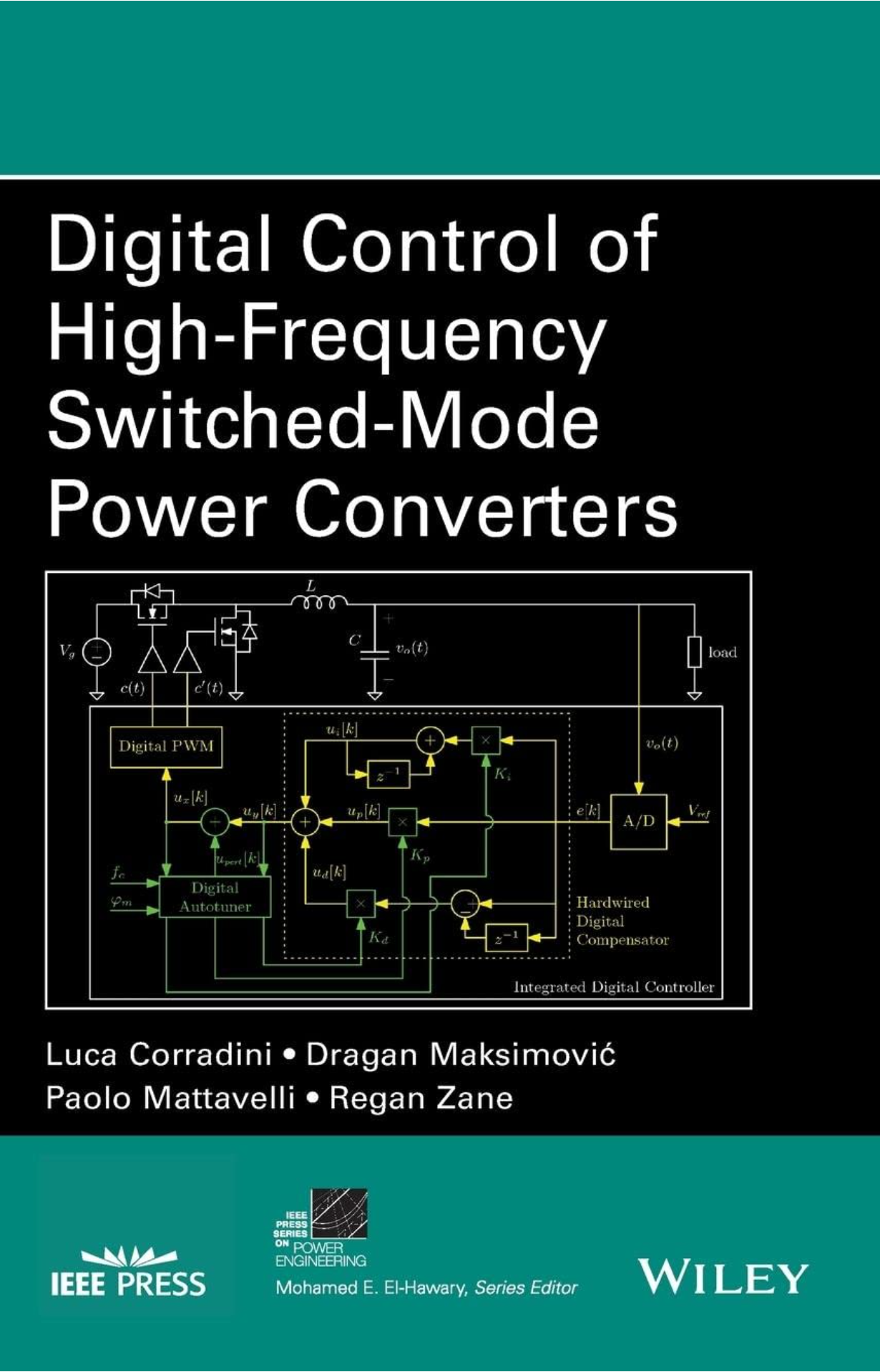
【教材】Digital Control of High-Frequency Switched-Mode Power Converters
【教材】Digital Control of High-Frequency Switched-Mode Power Converters
关于电源管理集成电路的综合资源,可在各个领域实现更高水平的功能和应用,并降低成本
完整版私信客服 186-6709-0885
【教材】Flip-Flop Design in Nanometer CMOS
【教材】Flip-Flop Design in Nanometer CMOS
电源管理集成电路设计是电源管理IC设计的综合参考资料,涵盖了主要电源管理电路的电路设计,如线性和开关模式稳压器,以及子电路,如功率开关、栅极驱动器及其电源、电平转换器、误差放大器、电流检测和控制环路设计。还涉及保护和诊断电路,以及物理设计方面,如横向和垂直功率传输、引脚排列、布局规划、接地/电源指南和封装。有一整章专门介绍集成无源器件的设计。本文阐述了电源管理集成电路(PMIC)在计算、物联网、移动和可再生能源等增长领域的应用。
完整版私信客服 186-6709-0885
【教材】Analog IC Design with Low-Dropout Regulators, Second Edition
【教材】Analog IC Design with Low-Dropout Regulators, Second Edition
最新模拟集成电路设计技术 《低压差稳压器模拟集成电路设计(第二版)》经过全面修订和扩展,以满足混合信号系统的新兴需求。本书教授模拟集成电路概念,并解释如何使用这些概念,采用双极型、CMOS和BiCMOS半导体工艺技术来设计、分析和构建线性低压差(LDO)稳压器集成电路。该书从所呈现的主题中汲取物理洞察力,并阐明如何为当今不断扩展的无线和移动市场开发和评估模拟集成电路。实用示例和章末复习题强化了这本前沿指南中开发的重要概念和技术。 学习如何: 评估电源系统 预测和规定线性稳压器的性能以及它们对电源、负载和其他工作条件变化的响应 使用半导体器件——电阻器、电容器、二极管和晶体管 组合微电子元件来设计电流镜、差分对、差分放大器、线性低压差稳压器及其变体 闭合和稳定用于调节电压和电流的反馈控制环路 设计建立可靠偏置电流和基准电路的电路 确定模拟集成电路和模拟系统的小信号动态特性 建立独立、稳定、无噪声且可预测的电源电压 实现过流、过热、反接电池和静电放电保护 测试、测量和评估线性稳压器集成电路
完整版私信客服 186-6709-0885
【教材】High Speed and Wide Bandwidth Delta Sigma ADCs
【教材】High Speed and Wide Bandwidth Delta Sigma ADCs
本书介绍了在纳米CMOS工艺中实现宽带宽(125MHz)过采样模数转换器(ADC)的技术。作者清晰完整地阐述了高速Δ-Σ调制器中的系统级挑战和实际设计解决方案。读者将能够将ADC实现为连续时间Δ-Σ(CT∆Σ)调制器,这种调制器提供简单的电阻输入,无需使用功耗大的输入缓冲器,并且具有固有的抗混叠特性,从而简化系统集成。作者专注于高速宽带宽ΔΣM的设计,这类设计在带宽范围上实现了突破,此前该带宽范围仅Nyquist转换器可实现。更具体地说,本书描述了面向GHz采样频率的ΔΣM的稳定性、功率效率和线性度限制。
完整版私信客服 186-6709-0885

【教材】Switching-Power-Supply-Design-and-Optimization_-2ed_-2014
【教材】Switching-Power-Supply-Design-and-Optimization_-2ed_-2014
《开关电源设计与优化》(第二版)全面修订,涵盖了设计最先进电源的最新技术,包括谐振(LLC)转换器,该书详细阐述了如何为当今尖端电子产品设计可靠、高性能的开关电源。本书涵盖了现代拓扑结构和转换器,并提供了关于设计或选择带隙基准源、使用详细的新设计图表分析邻近效应的变压器设计、降压效率损耗拆解图、主动复位技术、拓扑形态以及细致的交流-直流前端设计流程等新信息。 这份更新后的资源包含综合反馈环设计的设计图表和数值示例,包括TL431,以及世界上首个针对宽输入谐振(LLC)转换器的自顶向下简化设计方法。本实用指南还包含了一个针对正激式和反激式转换器的分步比较设计流程。 新版涵盖: 电压基准DC-DC转换器:拓扑到配置 现代转换器、复合转换器及相关技术 间断导通模式 交流-直流电源转换中的综合前端设计 交流-直流应用中的拓扑 分接电感器(基于自耦变压器)转换器 为DC-DC转换器选择电感器 反激式和正激式转换器变压器设计 正激式和反激式转换器:逐步设计与比较 印刷电路板(PCB)和热管理 闭环控制:反馈与稳定性,包括TL431 实用电磁干扰(EMI)滤波器设计 反激式和正激式转换器中的复位技术 可靠性、测试和安全问题 解析与优化降压转换器效率 软切换介绍以及详细的LLC转换器设计方法(附带PSpice仿真) 实用电路、设计思路和元件常见问题解答
完整版私信客服 186-6709-0885
【教材】CMOS Receiver Front-ends for Gigabit Short-Range Optical Communications
【教材】CMOS Receiver Front-ends for Gigabit Short-Range Optical Communications
综述光通信,包括长途传输系统和专注于短距离的新兴应用 解释必要的基础知识,如数据信号的特性、影响接收器设计的系统要求以及接收器设计中的关键参数 涵盖光学CMOS接收器的完整设计流程,从光传输理论基础分析到针对千兆位传输的短距离应用的最终架构
完整版私信客服 186-6709-0885
【教材】Intuitive Analog Circuit Design 2nd Edition
【教材】Intuitive Analog Circuit Design 2nd Edition
请您提供需要翻译的正文内容,以便我按照要求进行翻译。
完整版私信客服 186-6709-0885
【教材】Design of Integrated Circuits for Optical Communications 2nd Edition
【教材】Design of Integrated Circuits for Optical Communications 2nd Edition
唯一一本全面涵盖高速输入输出、锁相环、时钟数据恢复和包括光通信在内的收发器设计的光通信集成电路书籍 对高速数据传输的需求不断增长,重振了光通信领域,推动了高速器件和电路设计的广泛研究。随着互联网的普及以及微处理器和存储器速度的提升,数据传输仍然是瓶颈,这促使人们致力于开发更快的通信信道。 《光通信用集成电路设计(第二版)》涉及光通信收发器的高速集成电路设计。 在深入理解光器件的基础上,本书阐述了关键构建模块的分析与设计,如跨阻放大器、限幅放大器、激光驱动器、锁相环、振荡器、时钟数据恢复电路和多路复用器。 这本畅销教材的第二版经过全面更新,包括: 面向学生和工程师的宽带电路教程 关于时钟数据恢复电路和多路复用器的全新独特内容 专门讲述突发模式光通信的章节 对光收发器新电路发展的详细研究 对CMOS技术近期实现的探讨 本书非常适合从事光通信高速电路设计以及更广泛的有线通信领域的高年级研究生和工程师。
完整版私信客服 186-6709-0885
【教材】Designing Control Loops for Linear and Switching Power Supplies
【教材】Designing Control Loops for Linear and Switching Power Supplies
环路控制是电子工程的一个重要领域,当今的专业人士需要掌握。本书注重实用性,不深入过多理论,而是聚焦于补偿或稳定特定控制系统真正需要了解的知识。你可以直接查阅实用章节,其中包含大量设计示例和现成公式,以帮助你开展现场项目。你还能了解控制环路的基础和原理,从而更全面地理解相关内容。这本权威著作阐述了如何进行控制系统分析,并提供了关于实用补偿器的详细信息。它帮助你对系统进行测量,展示如何验证原型是否稳定以及是否具备足够的设计裕量。此外,你还将学习如何通过经过实验台验证的安全裕量来确保大批量生产。
完整版私信客服 186-6709-0885

【教材】Operational Amplifier Noise
【教材】Operational Amplifier Noise
集成MOS、MOM和MIM电容器,集成电感器
完整版私信客服 186-6709-0885
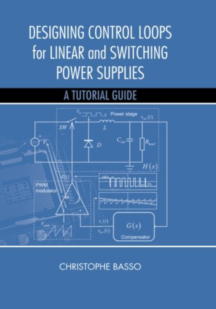
【教材】Designing Control Loops for Linear and Switching Power Supplies
【教材】Designing Control Loops for Linear and Switching Power Supplies
环路控制是电子工程的重要领域,当今专业人士必须掌握。本书不深入大量理论,而是专注于为给定控制系统进行补偿或稳定所需的实用知识。您可以直接查阅包含众多设计示例和现成公式的实用章节,以帮助您开展现场项目。您还将了解控制环路的基础和原理,从而更全面地理解相关内容。这本权威著作阐述了如何进行控制系统分析,并提供了有关实用补偿器的详细信息。它帮助您对系统进行测量,展示如何验证原型是否稳定以及是否具有足够的设计余量。此外,您还将学习如何通过经过工作台验证的安全余量确保大批量生产。
完整版私信客服 186-6709-0885
【教材】Smart and Flexible Digital-to-Analog Converters (Analog Circuits and Signal Processing Book 0)
【教材】Smart and Flexible Digital-to-Analog Converters (Analog Circuits and Signal Processing Book 0)
《智能灵活的数模转换器》一书提出了电流舵数模转换器(DAC)灵活性和自校正的新概念与实现方法,这些方法能够满足广泛的功能和性能规格要求,同时大大减少了对制造工艺的依赖。本书从DAC单元元件的准确性角度分析了DAC的线性度。对众多不同的电流舵DAC校正方法进行了分类。该分类揭示了公开文献中尚不存在的方法。此外,本书还系统地分析了针对各种DAC失配误差的自校准校正方法。例如,识别出DAC二进制电流的高效校准是一项重要的缺失方法。本书进一步提出了一种新方法,用于校正名义上相同的单位DAC电流和缩放二进制DAC电流的失配误差。提出了DAC灵活性的新概念。相关架构基于模块化设计方法,该方法使用并行子DAC单元来实现灵活的设计、功能和性能。通过使用250纳米、180纳米和40纳米标准CMOS中的三个DAC测试芯片,在实践中展示了自校正和灵活性这两个主要概念。对于该领域的资深专业人士和新手而言,《智能灵活的数模转换器》一书都将大有裨益。资深专业人士将找到从概念层面的分析到测试芯片层面的测量结果都经过充分阐述的新方法。该领域的新手将找到结构化的知识,其中包含全面引用的最先进方法以及许多经过充分解释的新颖内容。
完整版私信客服 186-6709-0885
【教材】Low-Power High-Resolution Analog to Digital Converters Design, Test and Calibration
【教材】Low-Power High-Resolution Analog to Digital Converters Design, Test and Calibration
随着CMOS制造技术的快速发展,越来越多的信号处理功能在数字域实现,以实现更低的成本、更低的功耗、更高的良率和更高的可重构性。这最近产生了对低功耗、低电压模数转换器的巨大需求,这些转换器可以在主流深亚微米CMOS技术中实现。然而,光刻波长与电路特征尺寸之间的差异正在增大。更低的电源电压显著降低了噪声容限,并增加了工艺、器件和设计参数的变化。因此,精确控制制造过程以保持均匀性变得越来越困难。纳米尺度制造中所用材料的固有随机性意味着性能将越来越多变,不仅在芯片之间,而且在每个芯片内部。参数变化将因纳米级集成电路的退化而加剧,导致参数随时间不稳定,最终导致故障的产生。工艺变化无法通过提高制造公差来解决;为了继续缩小尺寸,必须通过新的器件技术减少变化或通过设计进行管理。同样,芯片内性能变化也给测试方法带来了新的挑战。 为了解决这些问题,低功耗高分辨率模数转换器特别关注:i) 分别通过探索低压模拟设计和校准技术的潜力,提高高速、低杂散频谱模数转换性能的功率效率;ii) 开发电路技术和算法,以增强测试和调试潜力,动态检测错误,隔离和限制故障,并持续恢复错误。所描述方法的可行性已通过在标准180nm、90nm和65nm CMOS技术中制造的硅原型的测量得到验证。
完整版私信客服 186-6709-0885
【教材】Advanced Materials for Thermal Management of Electronic Packaging
【教材】Advanced Materials for Thermal Management of Electronic Packaging
随着热挑战成为电子行业持续提升器件和系统性能能力的障碍,电子封装中对先进热管理材料的需求已得到广泛认可。随着对更小、功能更强、效率更高的电子功率器件性能要求的提高,从有源电子扫描雷达阵列到网络服务器等各种系统都需要能够高效散热的组件。这要求材料具备高散热能力,并与芯片和电子封装保持兼容性。为满足关键需求,主动和被动冷却用热管理材料及技术取得了革命性进展,有望提供可集成且经济高效的热管理解决方案。本书满足了电子封装中先进热管理综合方法的需求,涵盖传热基础、组件设计指南、材料选择与评估、空气、液体和热电冷却、表征技术与方法、加工制造技术、成本与性能之间的平衡以及应用领域。最后一章介绍了电子封装用先进热管理材料发展的路线图和未来展望。
完整版私信客服 186-6709-0885
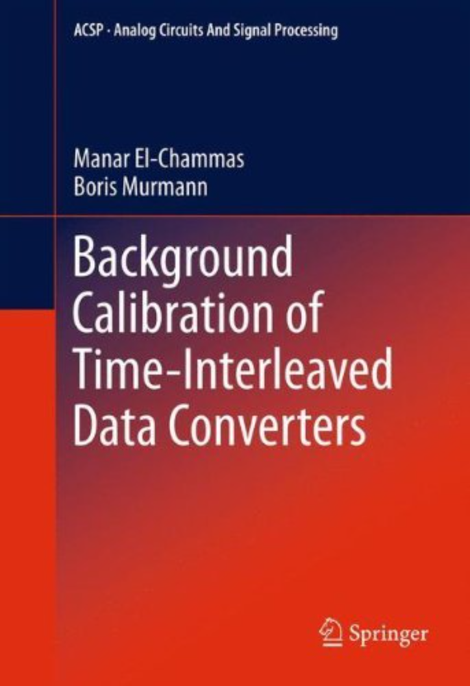
【教材】Background Calibration of Time-Interleaved Data Converters
【教材】Background Calibration of Time-Interleaved Data Converters
本书介绍了通过对多个模数数据转换器进行时间交织来满足严苛带宽要求的技术。读者将从可用于实际产品的低功耗解决方案的介绍中获益,同时减轻在实施此类系统架构时通常会出现的时变信号伪影。
完整版私信客服 186-6709-0885
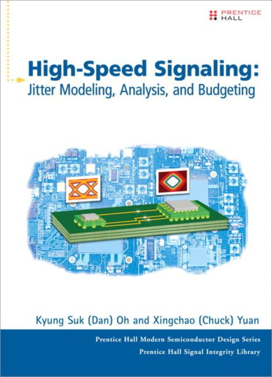
【教材】High-Speed Signaling: Jitter Modeling, Analysis, and Budgeting (Prentice Hall Modern Semiconductor Design Series)
【教材】High-Speed Signaling: Jitter Modeling, Analysis, and Budgeting (Prentice Hall Modern Semiconductor Design Series)
优化高速接口信号/电源完整性的新系统级技术——来自Rambus、斯坦福大学、伯克利分校和麻省理工学院的开拓性创新者 随着数据通信速率加速进入多吉赫兹范围,确保芯片内外的信号完整性已变得至关重要。信号完整性不能再仅通过改进封装或板级设计来解决:不同的工程团队必须从最早的设计阶段就紧密合作,以确定最佳的系统级解决方案。在《高速信号传输》中,该领域几位最受尊敬的从业者和研究人员介绍了用于应对这一挑战的尖端建模、仿真和优化技术。 由开拓性专家Dan Oh博士和Chuck Yuan博士编辑,这些撰稿人解释了为什么噪声和抖动不再可分离,展示了如何对它们日益复杂的相互作用进行建模,并全面介绍了一种新的仿真方法,以前所未有的精度预测链路级性能。 作者们从架构到大规模生产全面探讨信号完整性,深入讨论设计、实现和验证。内容包括: 无源通道建模、电源噪声和抖动建模以及系统裕量预测的新进展 平衡系统电压和时序预算以提高大批量制造中系统稳健性的方法 用于转换关键网络参数的实用、稳定公式 互连宽带建模中难题的改进解决方案 用于优化通道性能的均衡技术 关于抖动和时钟拓扑之间关系的重要新见解 用于现场链路性能测试的新型片上测量技术 信号完整性工程的趋势和未来方向 《高速信号传输》全面介绍了Rambus和其他领先高科技公司及大学开创的新技术:这些方法以前从未以如此多的实用细节呈现过。它对于所有关注信号完整性的人员都将是宝贵的资源,包括信号和电源完整性工程师、高速I/O电路设计师以及系统级板设计工程师。
完整版私信客服 186-6709-0885
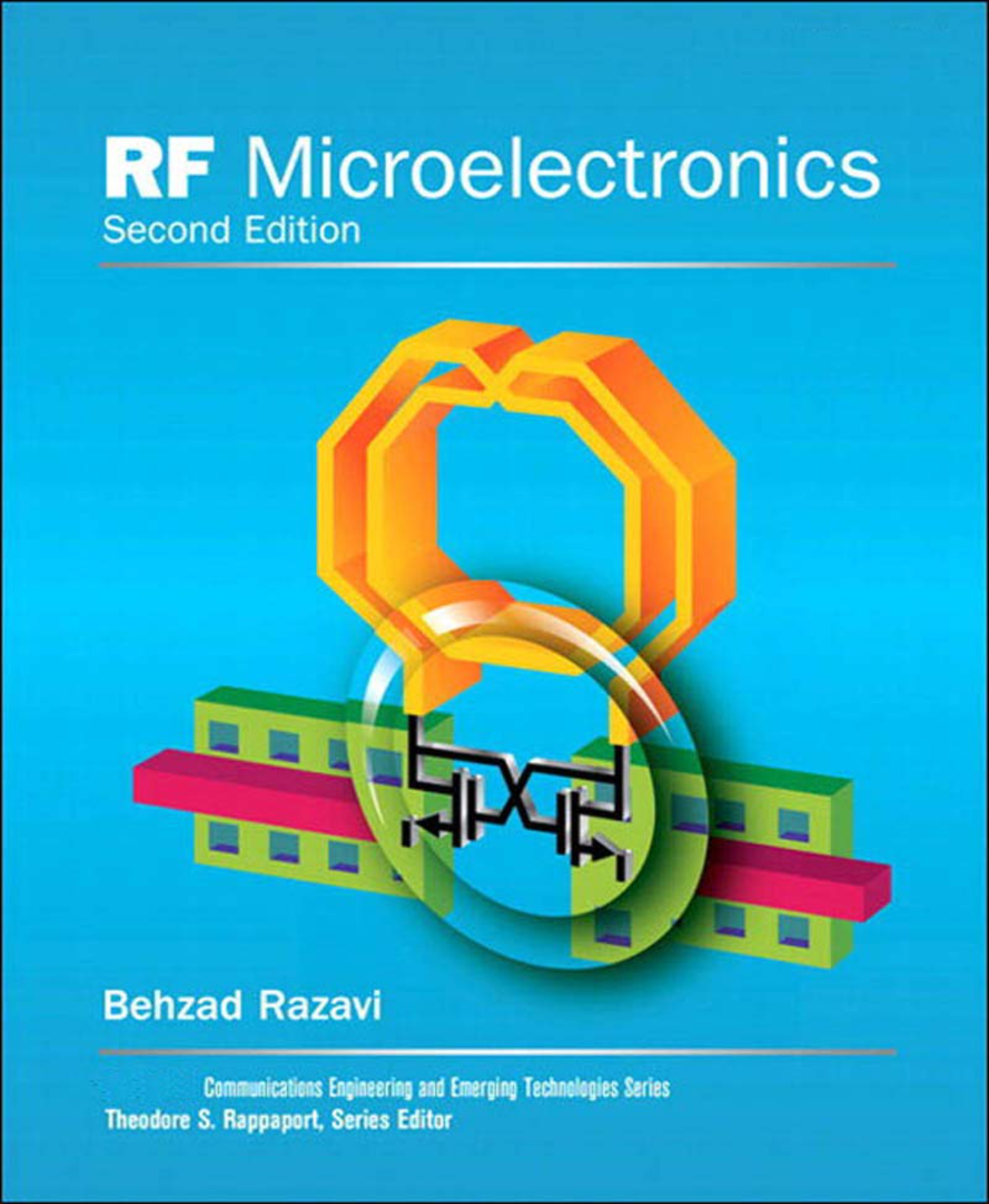
【教材】RF Microelectronics (Prentice Hall Communications Engineering and Emerging Technologies) 2nd Edition
【教材】RF Microelectronics (Prentice Hall Communications Engineering and Emerging Technologies) 2nd Edition
直流特性和直流相关电路设计,包括电源效率、线路和负载调节、误差放大器、压差以及功率晶体管尺寸确定
完整版私信客服 186-6709-0885
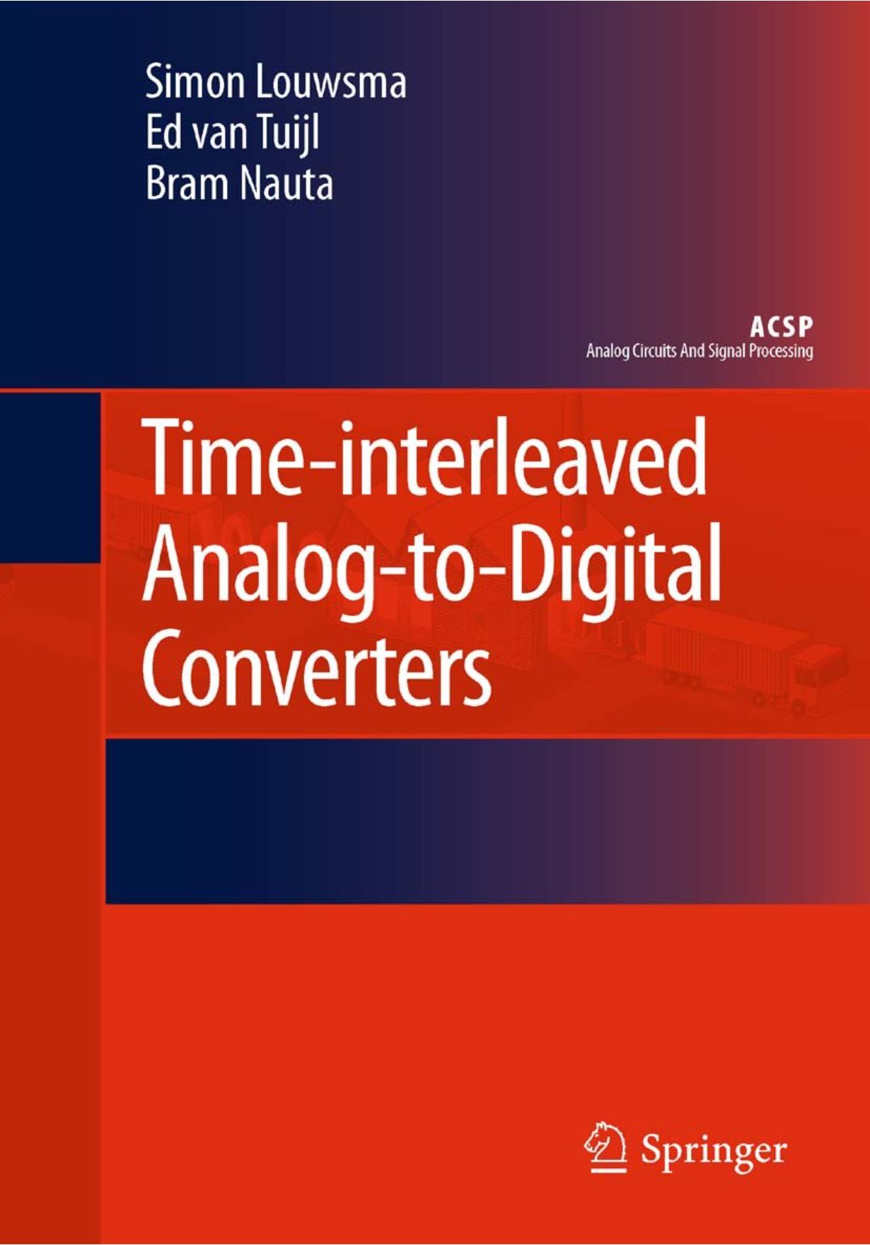
【教材】Time-interleaved Analog-to-Digital Converters
【教材】Time-interleaved Analog-to-Digital Converters
时间交错模数转换器描述了对低功耗时间交错模数转换器的研究。对时间交错跟踪保持电路进行了详细的理论分析,因为它必须能够处理GHz范围内的信号,且失真小、功耗低。时序校准并不理想,因此提出了不需要时序校准的设计技术。 通过对逐次逼近转换器和流水线转换器的理论分析,解决了高效功率子模数转换器的设计问题。结果表明,前者的功耗大约是后者的1/10,这一结论得到了文献的支持。 时间交错模数转换器描述了高性能时间交错模数转换器的设计,重点关注实际设计方面,面向工业界和研究领域。测量结果显示其性能达到同类最佳,采样率为1.8 GS/s,有效位数为7.9,功率效率为1皮焦/转换步。
完整版私信客服 186-6709-0885
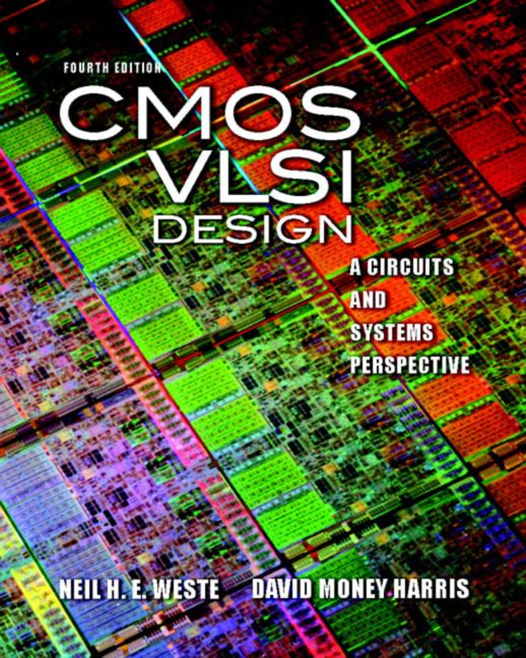
【教材】CMOS VLSI Design A Circuits and Systems Perspective 4th Edition
【教材】CMOS VLSI Design A Circuits and Systems Perspective 4th Edition
《CMOS VLSI设计:电路与系统视角》第四版全面且深入地涵盖了现代CMOS VLSI设计的整个领域。作者凭借丰富的行业经验和课堂教学经验,介绍了当今最先进、最有效的芯片设计实践。他们广泛更新了VLSI设计的每个关键要素的内容,并通过65纳米工艺示例阐明了最新的设计挑战。本书包含无与伦比的电路级内容,以及丰富的问题和实例,为各级读者提供了深刻的实践见解。
完整版私信客服 186-6709-0885
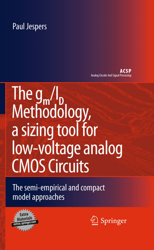
【教材】The gm_ID Methodology, a sizing tool for low-voltage analog CMOS Circuits
【教材】The gm_ID Methodology, a sizing tool for low-voltage analog CMOS Circuits
优化考虑封装、布局规划、电磁干扰、引脚分配、印刷电路板设计和热设计的物理设计
完整版私信客服 186-6709-0885
【教材】switching power supply design
【教材】switching power supply design
《开关电源设计》作为电源设计领域的权威指南,已在全球范围内得到认可,并已更新至第三版,涵盖了技术、材料和组件方面的最新创新。第三版介绍了所有常用拓扑结构的基本原理,为您提供设计尖端电源所需的基本信息。 本专家资源采用教程式、指导性的方法,包含大量设计示例、方程和图表。《开关电源设计》第三版具有以下特点: 适用于所有最实用的开关电源拓扑结构的设计 解决日常设计问题所需的基本原则 对磁学设计的高度关注 本版新增内容:一整章关于扼流圈设计和准谐振切换方法的内容 获取设计完整开关电源所需的一切 • 基本开关稳压器 • 推挽式和正激式转换器拓扑结构 • 半桥和全桥转换器拓扑结构 • 反激式转换器拓扑结构 • 电流模式和电流馈电拓扑结构 • 其他拓扑结构 • 变压器和磁性设计 • 高频扼流圈设计 • 双极型功率晶体管基极驱动 • MOSFET功率晶体管和输入驱动电路 • 磁放大器后置稳压器 • 开关损耗和缓冲电路 • 反馈环路稳定 • 谐振转换器 • 波形 • 功率因数、功率因数校正 • 荧光灯用高频电源 • 笔记本电脑和便携式电子设备用低输入电压稳压器 • 移相零电压过渡全桥转换器
完整版私信客服 186-6709-0885
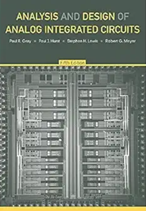
【教材】Analysis and Design of Analog Integrated Circuits, 5th Edition
【教材】Analysis and Design of Analog Integrated Circuits, 5th Edition
这是市场上唯一一本面向工程师的全面书籍,涵盖CMOS和双极型模拟集成电路的设计。第五版保留了其完整性,并更新了双极型和CMOS电路的内容。
完整版私信客服 186-6709-0885
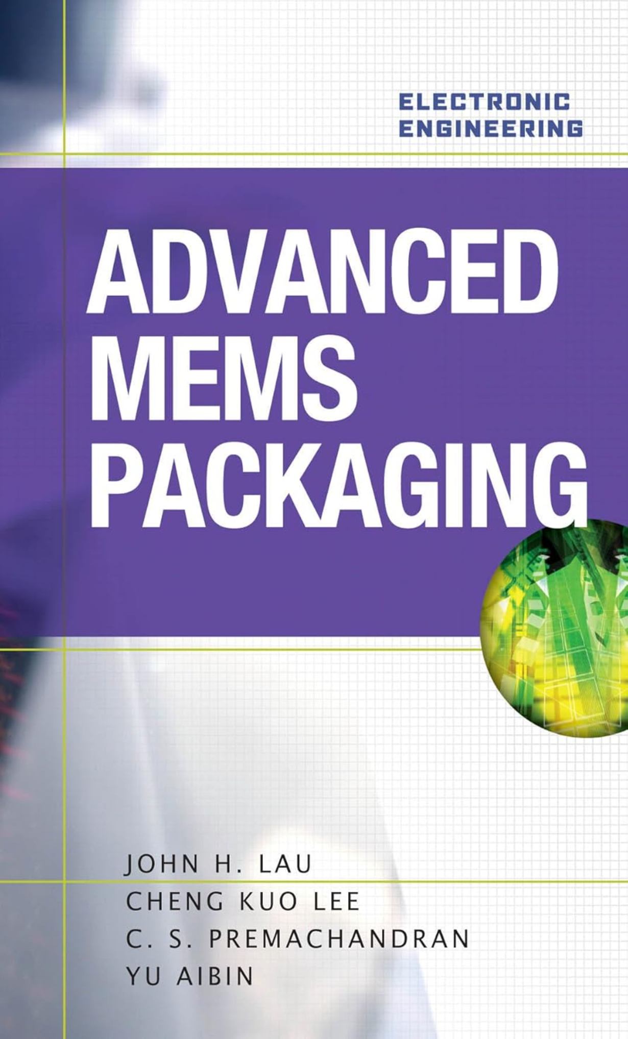
【教材】Advanced MEMS Packaging
【教材】Advanced MEMS Packaging
3D MEMS封装方法与解决方案综合指南 由该领域专家撰写的《先进MEMS封装》是那些面临MEMS器件及封装日益增长的关注所带来的挑战的人士的宝贵参考资料。这份权威指南介绍了前沿的MEMS(微机电系统)封装技术,如低温C2W和W2W键合以及3D封装。 这一权威资源帮助您为MEMS器件选择可靠、创新、高性能、坚固且经济高效的封装技术。本书还将有助于推动电气、光学、机械和热设计以及材料、工艺、制造、测试和可靠性方面的进一步研究与开发。探讨的主题包括: 先进IC和MEMS封装趋势 MEMS器件、商业应用和市场 超过360项MEMS封装专利和10种3D MEMS封装设计 用于3D MEMS封装的TSV MEMS晶圆减薄、切割和处理 低温C2C、C2W和W2W键合 符合RoHS标准的MEMS封装的可靠性 微加工和水键合技术 驱动机制和集成微加工 气泡开关、光开关和VOA MEMS封装 测辐射热计和加速度计MEMS封装 生物MEMS和生物传感器MEMS封装 射频MEMS开关、可调谐电路和封装
完整版私信客服 186-6709-0885
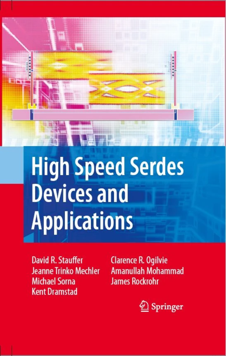
【教材】High Speed Serdes Devices and Applications
【教材】High Speed Serdes Devices and Applications
提供关于高速串行(HSS)设备通常具备的特性和功能的信息 解释高速串行(HSS)设备在协议应用中的使用方式 描述与设计和分析参考时钟分配网络相关的特性、功能和注意事项 包括如何测试高速串行(HSS)硬件和分析信号完整性的信息 讨论与高速串行(HSS)内核设计套件相关的特殊主题
完整版私信客服 186-6709-0885
【教材】The Designer's Guide to Jitter in Ring Oscillators
【教材】The Designer's Guide to Jitter in Ring Oscillators
强调时域应用中的抖动,因此无需从频域进行转换 为在性能以时域指定的应用领域中进行设计提供更直接的结果路径 包括振荡器类型的分类和现有研究文献的详尽指南,使设计人员能够找到合适的出版物以获取更详细的设计指导 涵盖测量技术的分类,以帮助设计人员了解如何验证电路设计的最终性能
完整版私信客服 186-6709-0885
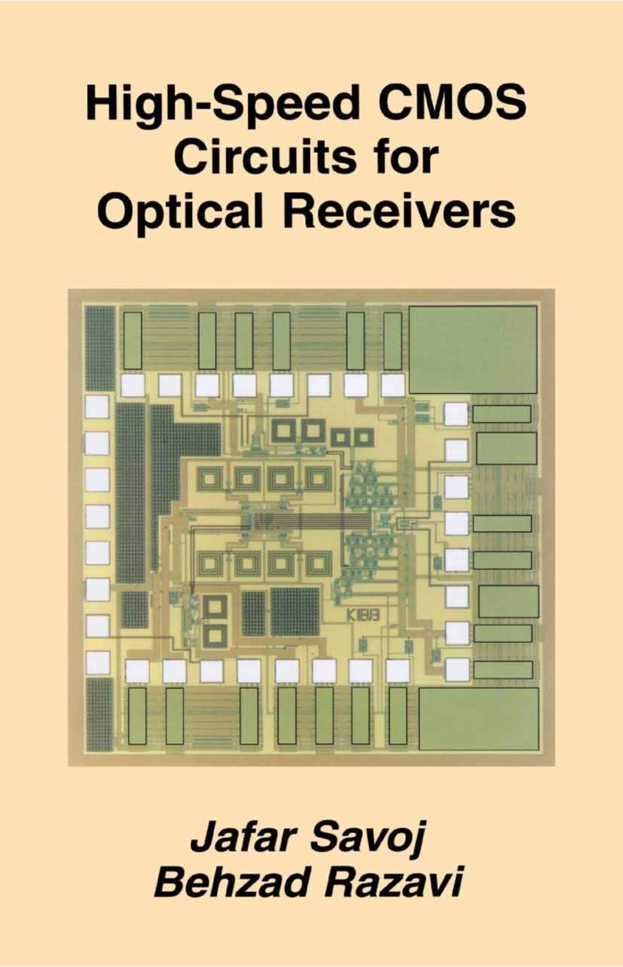
【教材】High-Speed CMOS Circuits for Optical Receivers 2001st Edition
【教材】High-Speed CMOS Circuits for Optical Receivers 2001st Edition
随着互联网节点数量的指数级增长,骨干网上传输的数据量也呈现出相同的增长趋势。全球互联网骨干网的负载很快将增加到每秒数十太比特。这表明骨干网带宽需求每七年将增长50到100倍。如此大量的数据传输需要低损耗、高带宽的合适介质。在现有的传输介质中,光纤在损耗和带宽方面性能最佳。高速数据可以在数百公里的单模光纤上传输,而不会显著损失信号完整性。这些光纤的成本不断降低,性能也在逐步提升。与此同时,光网络中使用的电子接口无法充分利用光纤的极限带宽,从而限制了网络的吞吐量。为了提高骨干网的数据速率,人们在系统和电路层面都提出了不同的解决方案。系统级解决方案基于波分复用(WDM)技术,利用不同颜色的光同时传输多个序列。与此同时,人们也投入了大量精力,通过高度发达的制造工艺和新颖的电路技术来提高电子收发器的工作速率。
完整版私信客服 186-6709-0885
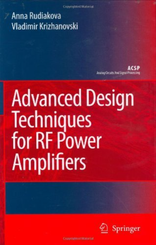
【教材】Advanced Design Techniques for RF Power Amplifiers (Analog Circuits and Signal Processing)
【教材】Advanced Design Techniques for RF Power Amplifiers (Analog Circuits and Signal Processing)
《射频功率放大器先进设计技术》的主要目的是为读者深入分析射频高效功率放大器的理论方面、建模和设计策略。《射频功率放大器先进设计技术》首先对当前问题的现状进行了分析回顾。然后,它转向对接近过渡频率的BJT(双极结型晶体管)F类功率放大器的理论分析,并提出了必要的实现条件。下一部分关注理论结果的实践验证和演示。随后是专门讨论高效功率放大器输出网络的部分。提出了一种新型光子带隙结构,该结构在通带和阻带中均提供了改进的特性。最后,基于上述结构,提出了五次谐波峰化F类功率放大器的设计。
完整版私信客服 186-6709-0885
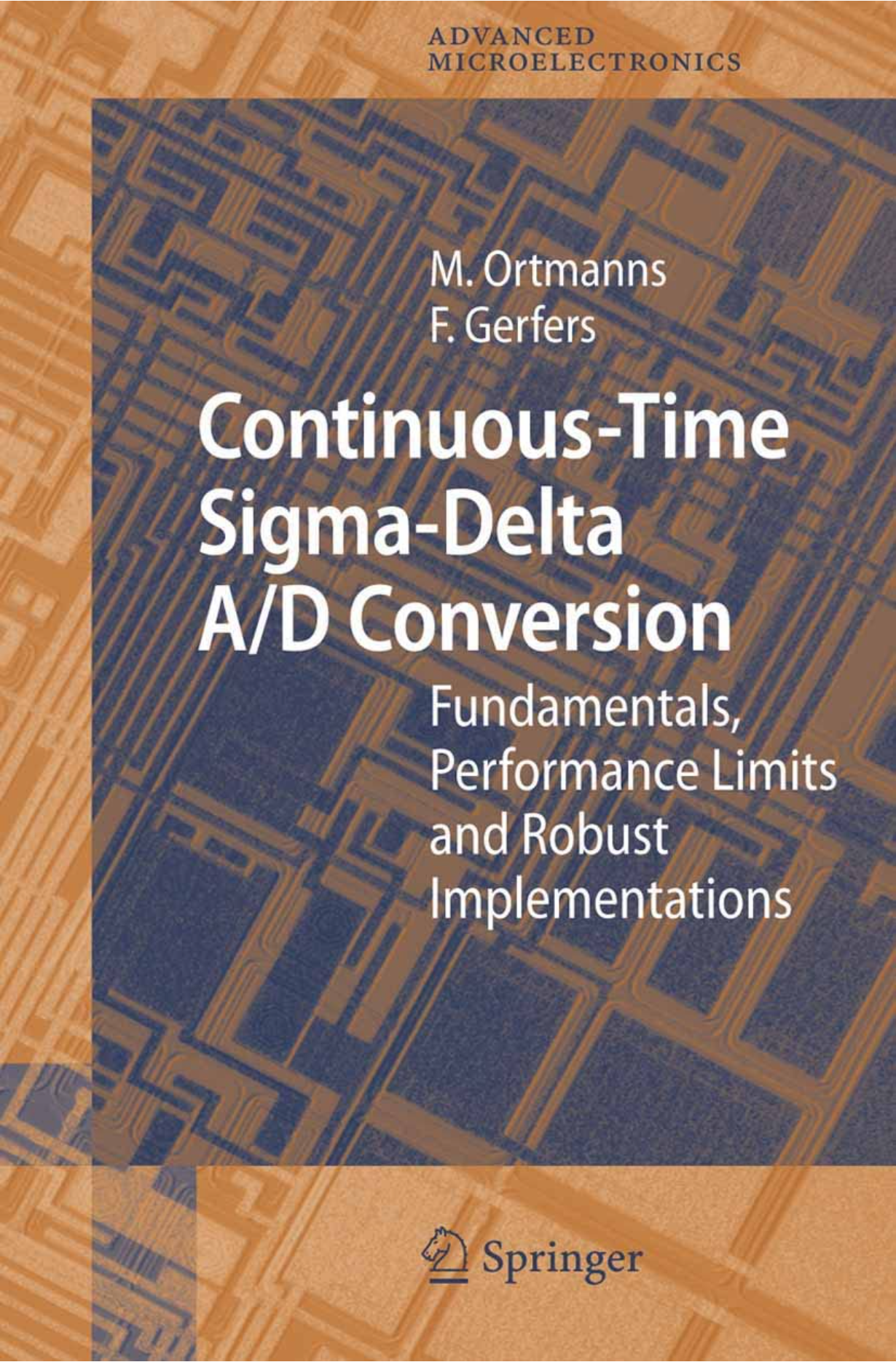
【教材】Continuous-Time Sigma-Delta A/D Conversion: Fundamentals, Performance Limits and Robust Implementations
【教材】Continuous-Time Sigma-Delta A/D Conversion: Fundamentals, Performance Limits and Robust Implementations
Σ-Δ模数转换器是无线和多媒体应用中的关键构建模块。本书内容全面,涵盖了Σ-Δ调制器连续时间(CT)实现的分析、设计和仿真过程中出现的所有相关方面。书中包含了作者在CT Σ-Δ调制器领域多年研究的成果,包括不同CT调制器架构的分析与建模、CT/数字时间(DT)环路滤波器综合、所有组件的详细误差分析,以及针对CT Σ-Δ调制器中非理想行为的潜在补偿/校正方案。此外,本书还提供了实现低功耗的指导以及多种实用实现方法。书中证明,所有提出的新理论、架构和可能的校正技术均已通过离散电路或集成电路的测量得到验证。同时,本书还提供了定量结果,从而能够预测最终的精度。
完整版私信客服 186-6709-0885
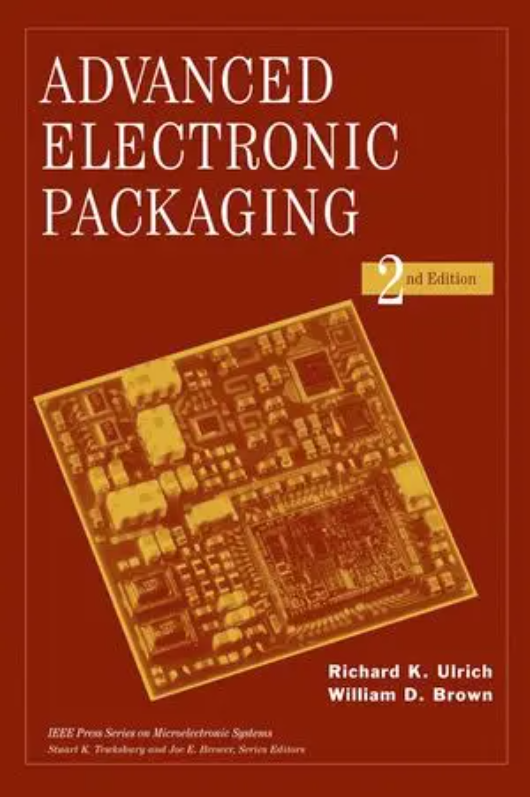
【教材】Advanced Electronic Packaging
【教材】Advanced Electronic Packaging
《先进电子封装(第二版)》反映了电子封装行业的变化,以及自1999年第一版出版以来学生、工程师和教育工作者的反馈。与第一版一样,每章均由一位或多位公认的专家撰写,然后经过仔细编辑,以确保全书质量和方法的一致性。 熟悉第一版的读者会注意到几个关键变化。例如,有机基板和陶瓷基板现在分章介绍。新增了关于无源器件、射频和微波封装、电子封装组装以及成本评估与组装的章节。此外,读者还能获取以下主题的最新信息和研究成果: 封装材料及应用 建模与仿真 材料分析技术 MEMS封装 制造技术与封装设计 可靠性 电气、机械和热学考量 三维封装 第一版的所有特点都得到了保留,该书已成为行业标准和受欢迎的研究生教材。实例阐释了实际应用,并通过大量练习加以强化,使读者能够将新获得的知识付诸实践。此外,书中还提供了参考文献,引导读者获取更深入的信息和专业主题的主要资源。 经过全面更新,这本综合性参考书仍然是该领域卓越的研究生教材,也是工程师和科学家的必备参考资料。
完整版私信客服 186-6709-0885
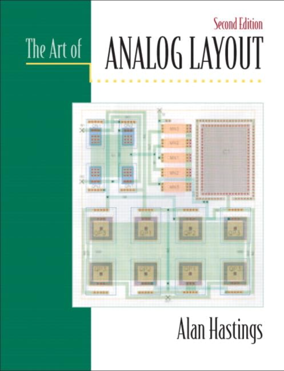
【教材】Art of Analog Layout, The 2nd Edition
【教材】Art of Analog Layout, The 2nd Edition
适用于模拟布局的电气工程课程或专业布局设计师。 本文涵盖了成功设计模拟集成电路布局所涉及的问题。黑斯廷斯提供了清晰的指导,没有强调布局的理论物理或数学分析。与更常见的器件几何和 schematic 表示相比,他强调器件的横截面和基于载流子的器件操作模型。
完整版私信客服 186-6709-0885

【教材】The Designer’s Guide to Verilog-AMS
【教材】The Designer’s Guide to Verilog-AMS
Verilog硬件描述语言(Verilog-HDL)长期以来一直是描述复杂数字硬件最流行的语言。它最初是一种专有语言,但由Cadence设计系统公司捐赠给设计社区,作为开放标准的基础。该标准于1995年由IEEE在1364-1995标准中正式确立。大约在同一时期,一个名为模拟Verilog国际的小组成立,旨在提议对Verilog进行扩展,以支持模拟和混合信号仿真。该小组的初步成果于1996年问世,当时发布了Verilog-A的语言定义。Verilog-A并非旨在直接与Verilog-HDL协同工作,而是一种具有相似语法和相关语义的语言,旨在对模拟系统进行建模,并与SPICE类电路仿真引擎兼容。Verilog-A的首个实现很快跟进:Cadence推出了一个可在其Spectre电路模拟器上运行的版本。随着更多Verilog-A实现的出现,负责定义Verilog模拟和混合信号扩展的小组继续开展工作,并于2000年发布了Verilog-AMS的定义。Verilog-AMS结合了Verilog-HDL和Verilog-A,并添加了额外的混合信号构造,提供了一种适用于模拟、数字和混合信号系统的硬件描述语言。同样,Cadence率先发布了这种新语言的实现,其产品名为AMS Designer,该产品结合了他们的Verilog和Spectre仿真引擎。
完整版私信客服 186-6709-0885
【教材】Power Electronics: Converters, Applications, and Design 3rd Edition
【教材】Power Electronics: Converters, Applications, and Design 3rd Edition
控制环路设计和PWM生成,确保稳定性和快速瞬态响应;电流模式控制中的次谐波振荡(斜率补偿的分析与电路设计)
完整版私信客服 186-6709-0885
【教材】Power Electronics: Converters, Applications, and Design 3rd Edition
【教材】Power Electronics: Converters, Applications, and Design 3rd Edition
控制环路设计和PWM生成,确保稳定性和快速瞬态响应;电流模式控制中的次谐波振荡(斜坡补偿的分析与电路设计)
完整版私信客服 186-6709-0885
【教材】Voltage References: From Diodes to Precision High-Order Bandgap Circuits
【教材】Voltage References: From Diodes to Precision High-Order Bandgap Circuits
关于集成电压基准设计的最重要教程资源,从理论到实际应用。 《电压基准》涵盖了可市场化和精密集成电压基准背后的概念历史和实际设计问题范围。本书对专业人士有效,对新手设计师也易于理解,提供了对简单基础设计以及精密最先进设计的熟悉度。还涵盖了片上系统(SOC)解决方案以及低电压、低功耗和噪声混合信号环境的设计影响。通过设计示例增强,本卷将增加读者对模拟集成电路以及生产商业上可销售和可靠器件所涉及问题的理解。 主要主题包括: 集成电压基准的完整设计 电压基准基础,从二极管和电流镜到温度相关电流基准 零阶、一阶、二阶和高阶基准电路的设计 最先进的曲率校正技术 集成基准的实际设计问题,从误差源和电路拓扑到微调电路、封装偏移效应和表征 《电压基准》是集成电路设计师、产品工程师、测试工程师、研究人员和教授以及本科生和研究生的必备书籍。
完整版私信客服 186-6709-0885
电磁兼容(EMC)技术应用于硬件安全芯片设计
电磁兼容(EMC)技术应用于硬件安全芯片设计
本演讲深入探讨了电磁兼容(EMC)技术与硬件安全之间的紧密联系,重点介绍了如何利用EMC合规性测试技术来评估和提升集成电路芯片的安全性。演讲内容涵盖EMC基础概念(电磁干扰EMI与电磁抗扰度EMS)、标准化IC芯片测试方法(如磁环探头法、RF-DPI注入法),以及这些技术如何转化为侧信道攻击分析工具。核心部分详细讲解了芯片-封装-系统(CPS)协同仿真技术,特别是芯片电源模型(CPM)的构建方法,包括被动网络提取与主动功耗电流建模。通过AES加密引擎的实际案例,展示了如何仿真分析功耗相关侧信道泄漏,并在设计阶段评估不同防护技术的有效性,为硬件安全设计提供了系统性的方法论指导。
完整版私信客服 186-6709-0885
【教材】Dynamic Analysis of Switching-Mode DC_DC Converters
【教材】Dynamic Analysis of Switching-Mode DC_DC Converters
现代开关电源最关键的部分是稳压DC/DC转换器。其动态行为直接决定或影响电源的四个重要特性:•反馈环路的稳定性•输入电压纹波抑制以及与之密切相关的对输入电压扰动的瞬态响应•输出阻抗以及与之密切相关的对负载扰动的瞬态响应•与输入EMI滤波器的兼容性由于转换器工作的复杂性,预测其动态行为并非易事。如果没有准确的预测,仅依靠构建电路并对其进行调整直到工作满意,工程成本很容易上升,并且可能会错过进度。当使用SPICE等通用电路仿真程序在计算机中构建电路时,情况也并没有好多少。(本书末尾有一张表格,用于获取一个特别适合开关模式功率转换器动态分析的计算机程序的信息:DYANA,是“动态分析”的首字母缩写。DYANA基于本书中给出的方法。)本书的主要目标是通过提供用户友好的分析工具、已完成分析的具体结果(为方便读者应用而制成表格)以及如何应用书中提供的工具的示例,帮助电源设计人员预测动态行为。
完整版私信客服 186-6709-0885